- ページ 5
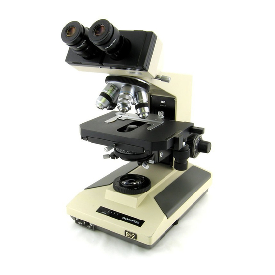
顕微鏡 Olympus BH-2 BHTのPDF マニュアルをオンラインで閲覧またはダウンロードできます。Olympus BH-2 BHT 24 ページ。 Sliding focus block
Olympus BH-2 BHT にも: 完全な分解、洗浄、再組み立て (23 ページ)

Filtered DC Power Supply
Diode D201 and capacitor C201 operate as a peak detector to produce filtered DC power from the full‐wave‐rectified
output of bridge rectifier DB101. This filtered DC power line supplies power to the comparators and their respective
LEDs. The AC ripple present on this line depends on the amount of current pulled by the comparators and LEDs. At
minimal commanded lamp intensity (i.e., with all four LEDs in the off state), very little current is required and the voltage
on this line is approximately +10.5V with little AC ripple. As the lamp intensity is increased (and the LEDs begin to
successively illuminate), the current drain on this line increases as does the resulting AC ripple. When the lamp is at
maximum intensity, all four LEDs are illuminated and the AC ripple is at its maximum, resulting in an average voltage on
the filtered DC power supply line of approximately +9.5V. Figure 25 shows the ripple voltage on the filtered DC power
supply line with the equipment operating under worst‐case ripple conditions of maximum lamp intensity. The green
trace is the positive output of bridge rectifier DB101 and the blue trace is the filtered DC power supply line.
Comparator Thresholds
The switching thresholds of the four op‐amp comparators are provided by a four‐stage voltage divider consisting of
resistors R208, R209, R210, R211, and R212. These thresholds are configured to allow the comparators to illuminate the
LEDs at pre‐defined lamp voltages of 2V, 4V, 6V, and 7V, in response to the decreasing control signal from the intensity
potentiometer. Figure 26 shows the threshold voltages on the inverting pins of the op‐amp comparators. The green
trace is the positive output of bridge rectifier DB101, from which the four threshold voltages are derived. The blue, red,
cyan, and magenta traces are the threshold voltages on the inverting inputs of IC1‐A, IC1‐D, IC1‐B, and IC1‐C,
respectively.
Control‐Signal Clamp
Resistors R213 and R214, and diodes D202, D203, and D204, clamp the voltage level of the intensity control signal from
potentiometer RV101 to keep the non‐inverting inputs of the comparators from ever dropping below approximately
+0.7V. This is necessary to prevent the LEDs from illuminating briefly during the intervals where both the wiper of
potentiometer RV101 and the comparator thresholds drop to zero at the zero crossings of the AC line. If both inputs to
the comparators were allowed to simultaneously drop to zero, the comparators would be in an indeterminate state, and
depending on the input‐offset voltage parameters of the specific op‐amp devices, their outputs could pull low during
these intervals, resulting in one or more LEDs not fully extinguishing when they should.
The operation of the control‐signal clamp is as follows. Resistor R214 feeds a DC current through the two series‐
connected silicon diodes, D203 and D204, producing a potential on the anode of diode D204 two diode drops above
ground (approximately +1.4V). The anode of diode D202 connects to this +1.4V node and its cathode connects to the
non‐inverting inputs of the four comparators. Resistor R213 couples the control signal from potentiometer RV101 to the
non‐inverting inputs of the comparators. Any time the control signal is low enough to forward bias diode D202, the
voltage on the non‐inverting inputs of the comparators is clamped to approximately +0.7V (i.e., one diode drop less than
+1.4V). As the voltage on the wiper of RV101 increases, diode D202 turns off and is effectively out of the circuit, thereby
providing no further clamping action. This mechanism allows the intensity control signal to swing positive without
restraint, but prevents it from dropping below approximately +0.7V.
Figure
27 shows the waveform of the clamped
control signal at the 50% setting of the intensity control, as measured at the non‐inverting inputs of the comparators.
Voltage Comparators
Integrated circuit IC1 is a NEC uPC324C quad operation amplifier. All four sections of IC1 are operated open‐loop as
voltage comparators and are configured to drive the four bar‐graph LEDs in response to the clamped control signal from
potentiometer RV101. Each comparator illuminates its associated LED by driving its output low during the intervals
where the clamped control signal drops below its threshold voltage, and extinguishes its LED by driving its output high
during the intervals where the clamped control signal exceeds its threshold voltage. Figure 28 shows the operation of
one of the comparators (IC1‐B) with the 6V LED illuminated. In these waveforms, the intensity control is set to the 70%
setting. The green waveform is the threshold voltage present on the inverting pin of IC1‐B, and the blue waveform is the
clamped control signal on the non‐inverting pin of IC1‐B. During the intervals where the control signal is below the
threshold voltage, the comparator output pulls low, illuminating the 6V LED, and during the intervals where the control
signal is clamped to approximately +0.7V (and is exceeding the threshold voltage), the comparator output pulls high,
Olympus BH‐2 (BHT/BHTU) Electronics
Revision 2
Page 5 of 24
