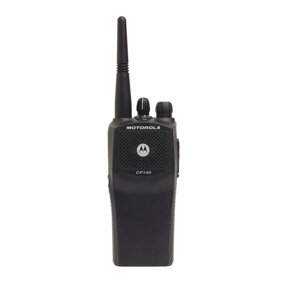
Motorola CP160 서비스 정보 - 페이지 16
{카테고리_이름} Motorola CP160에 대한 서비스 정보을 온라인으로 검색하거나 PDF를 다운로드하세요. Motorola CP160 46 페이지. Uhf2 (438-470mhz)
Motorola CP160에 대해서도 마찬가지입니다: 사용자 설명서 (46 페이지), 기본 사용 설명서 (16 페이지), 기본 사용 설명서 (16 페이지), 기본 사용 설명서 (18 페이지), 자세한 서비스 매뉴얼 (28 페이지), Cps/튜너 설치 매뉴얼 (6 페이지), 서비스 정보 (46 페이지)

2-8
4.2
Voltage Controlled Oscillator (VCO)
The VCOBIC (U251), shown in Figure 2-5, in conjunction with the Fractional-N synthesizer (U201)
generates RF in both the receive and the transmit modes of operation. The TRB line (U251 pin 19)
determines which oscillator and buffer are enabled. A sample of the RF signal from the enabled
oscillator is routed from U251 pin 12 through a low pass filter, to the prescaler input of the
synthesizer IC (U201 pin 32). After frequency comparison in the synthesizer, a resultant DC control
voltage is used to steer the VCO frequency. When the PLL is locked on frequency, this voltage can
vary between 3.5V and 10V. L251 and C252 further attenuate noise and spurs on the steering line
voltage.
In the receive mode, the TRB line (U251 pin 19) is low. This activates the receive VCO and the
receive buffer of U251, which operate within the range of 393.15 to 425.15 MHz. The VCO
frequency is determined by tank inductor L254, C253-C257, and varactor D251. The buffered RF
signal at U251 pin 8 is further amplified by Q280 and applied as RX_INJ to the low-pass injection
filter in the receiver front end circuit.
In the transmit mode, U251-19 is driven high by U201 pin 2, enabling the transmit VCO and buffer.
The 438-470 MHz RF signal from U251 pin 10 is applied as TX_INJ to the input of the transmitter
circuit via matching network C290-C291 and L291. TX VCO frequency is determined by L264,
C263-C267, and varactor D261. High-port audio modulation from the synthesizer IC is applied as
VCO_MOD to varactor D262 which modulates the transmit VCO.
NC
NC
V_SF (U201 Pin 28)
Steer Line
Voltage
(V_STEER)
RX
Tank
TX
Tank
Pin 20
Pin 7
Pin 13
Pin 3
Vcc-Superfilter
Collector/RF in
Pin 4
RX
Pin 5
RX VCO
Pin 6
Circuit
Pin 16
TX
TX VCO
Pin 15
Circuit
Vsens
Circuit
Pin 18
Vcc-Logic
3V
(U330 Pin 5)
Figure 2-5 UHF VCO Block Diagram
AUX3 (U201 Pin 2)
TRB_IN
Pin 19
TX/RX/BS
Switching Network
Presc
U251
VCOBIC
RX
Rx Active
Bias
Tx Active
TX
Bias
Pin 2
Pin 1
Pins 9,11,17
Rx-I adjust
Tx-I adjust
V_SF
(U201 Pin 28)
THEORY OF OPERATION
Prescaler Out
Pin 12
U201 Pin 32
Buffer
Q280
Pin 8
RX INJ
Pin 14
3V (U330 Pin 5)
VCC Buffers
Pin 10
Matching
Network
TX INJ
