Bose Personalized Amplification System Handbuch zur Fehlersuche - Seite 36
Blättern Sie online oder laden Sie pdf Handbuch zur Fehlersuche für Verstärken Bose Personalized Amplification System herunter. Bose Personalized Amplification System 50 Seiten.
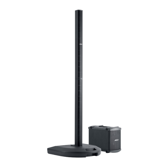
Auch für Bose Personalized Amplification System: Benutzerhandbuch (28 seiten)
4
3
2
1
A7
5
A6
6
A5
7
8
A4
32-lead PLCC
9
A3
Top View
10
A2
A1
11
A0
12
DQ0
13
14 15 16 17 18 19 20
29LE020 EEPROM Pinout Diagram
P
D
IN
ESCRIPTION
Sym bol
Pin Nam e
A
-A
Row Address Inputs
17
7
A
-A
Column Address Inputs
6
0
DQ
-DQ
Data Input/output
7
0
CE#
Chip Enable
OE#
Output Enable
WE#
Write Enable
V
Power Supply
DD
V
Ground
SS
NC
No Connection
F
B
UNCTIONAL
LOCK
A 17 - A 0
Address Buffer & Latches
CE#
OE#
WE#
APPENDIX
32 31 30
29
A14
28
A13
27
A8
26
A9
25
A11
24
OE#
23
A10
22
CE#
21
DQ7
Functions
To provide memory addresses. Row addresses define a page for a Write cycle.
Column Addresses are toggled to load page data
To output data during Read cycles and receive input data during Write cycles.
Data is internally latched during a Write cycle.
The outputs are in tri-state when OE# or CE# is high.
To activate the device when CE# is low.
To gate the data output buffers.
To control the Write operations.
To provide:
5.0V supply (4.5-5.5V) for SST29EE020
3.0V supply (3.0-3.6V) for SST29LE020
2.7V supply (2.7-3.6V) for SST29VE020
Unconnected pins.
29LE020 EEPROM Pinout Table
D
IAGRAM
X-Decoder
Control Logic
29LE020 EEPROM Block Diagram
1
2
-
+
3
-
+
4
TLO72, Dual Op-Amp
Y-Decoder and Page Latches
I/O Buffers and Data Latches
36
1. Output1
8
2. Inverting input1
3. Non-inverting input 1
7
4. -Vcc
5. Non-inverting input 2
6
6. Inverting input 2
7. Output 2
5
8. +Vcc
SuperFlash
Memory
DQ 7 - DQ 0