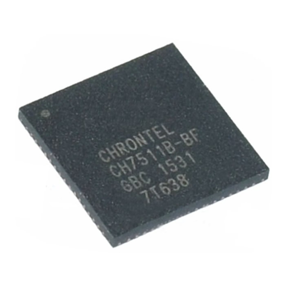
Chrontel CH7511B Design-Handbuch - Seite 8
Blättern Sie online oder laden Sie pdf Design-Handbuch für Empfänger Chrontel CH7511B herunter. Chrontel CH7511B 16 Seiten. Edp/dp receiver

CHRONTEL
• GPIO [0:3]
These pins can be used as panel select signals. They can be pulled high or low forming into 16 different combinations.
Every combination can match with one panel type. The connection is shown in Figure 9.
Method 1 (default)
GPIO [3:0] can be connected to high/low level by pull-up/pull-down resistors on the CH7511B/7512B PCB board;
The CH7511B/7512B can obtain the correct LVDS Panel selection value upon power ON or reset. As shown in
Figure 10, if the customer don't want to change MB, they can they the GPIO[0:3] in LCD inverter to identify
different panel.
8
SW 1
+3.3V
C1
R3
10K
0.1uF
SW 2
BLUP
BLUP
BLUP
BLUP
BLUP
BLUP
BLUP
R4
10K
C2
SW 3
0.1uF
C3
0.1uF
Figure 8: BLDN, BLUP and PWRDN Connections
U1
38
GPIO[3]
37
GPIO[2]
34
GPIO[1]
33
GPIO[0]
CH7511
Figure 9: GPIO [0:3] connections
+3.3V
R1
10K
BLDN
R2
10K
55
BLDN
56
BLUP
+3.3V
R5
41
PW RDN
10K
PW RDN
R6
10K
LVDD(+3.3V)
R1
R2
R3
R4
10K
10K
10K
10K
R5
R6
R7
R8
100
100
100
100
206-1000-014
AN-B014
CH7511
GPIO[3]
GPIO[2]
GPIO[1]
GPIO[0]
Rev. 1.7
2020-07-14
