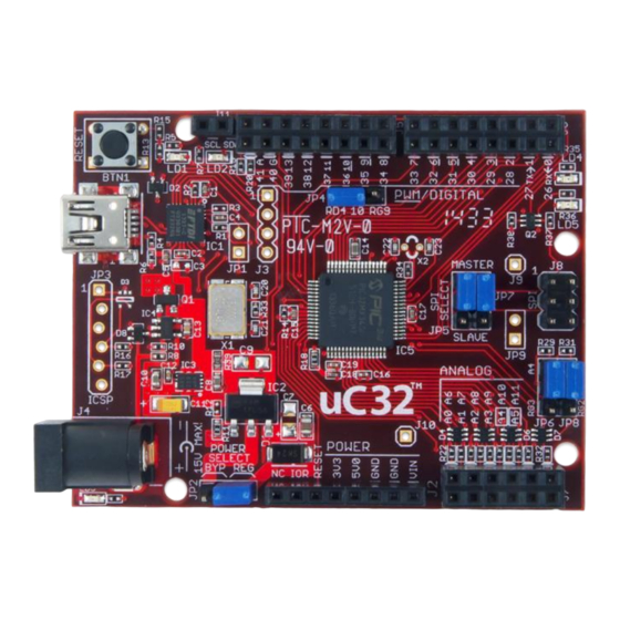
Digilent chipKIT uC32 Referenzhandbuch - Seite 7
Blättern Sie online oder laden Sie pdf Referenzhandbuch für Hauptplatine Digilent chipKIT uC32 herunter. Digilent chipKIT uC32 18 Seiten.

chipKIT™ uC32™ Board Reference Manual
For input voltages above 9V, the regulator will get extremely hot when drawing high currents. Both the NCP1117
and the LM1117 have output short circuit protection and internal thermal protection and will shut down
automatically to prevent damage.
The 3.3V regulator is a Microchip MCP1725. This regulator is rated for a maximum output current of 500mA. The
absolute maximum input voltage for the MCP1725 is 6V. This regulator has internal short circuit protection and
thermal protection. It will get noticeably warm when the current consumed by the VCC3V3 bus is close to the
500mA maximum.
The 5V power bus, VCC5V0, can be powered from one of three sources:
The USB5V0 bus when the board is operating under USB power
The output of the on-board 5V regulator when operating from an external 7V-15V supply
Directly from the external supply when operating from a regulated 5V external supply with jumper JP2 in
the BYP position
Switch-over from USB power to external power is done automatically and the external supply will be used if both
are present.
Jumper JP2 is used to route the external power supply voltage through the on-board 5V regulator or directly to the
VCC5V0 bus, bypassing the on-board 5V regulator. Normally, JP2 is in the REG position. This routes the external
supply through the 5V regulator. Operation from an externally regulated 5V supply is provided by placing the
jumper in the BYP position.
The forward drop across the MCP1725 is typically 210mV (350mV max) at 500mA output. With JP2 in the BYP
position, this will allow correct operation of the 3.3V power supply from an input voltage down to 3.5V. This lets
you power the board from batteries and other lower voltage power sources. In that case, the VCC5V0 power bus
will not be powered at 5V.
Note: When JP2 is in the BYP position, do not apply more than 6V to the external power input. This can destroy the
3.3V regulator and possibly the PIC32 microcontroller as well.
The PIC32 microcontroller is rated to use a maximum of 75mA of current when operating at 80 MHz. This allows up
to 425mA from the VCC3V3 bus and up to 925mA from the VCC5V0 bus to power external devices.
The POWER connector, J2, is used to power shields connected to the uC32 board. The following pins are provided
on this connector:
NC (pin 1): This pin is not used.
IOR (pin 2): Provides a 3.3v reference voltage to the shield which the shield should observe as the maximum
input pin voltage to the uC32.
P32_RST (pin 3): This connects to the MCLR pin on the PIC32 microcontroller and can be used to reset the PIC32.
VCC3V3 (pin 4): This routes the 3.3V power bus to shields. This pin can provide ~425mA.
VCC5V0 (pin 5): This routes the 5V power bus to shields. This pin can provide up to ~900mA to shields, however,
the total provided by pins 2 and 3 shouldn't exceed 925mA.
GND (pin 6, 7): This provides a common ground connection between the uC32 and the shields.
VIN (pin 8): This connects to the voltage provided at the external power supply connector. This can be used to
provide unregulated input power to the shield. It can also be used to power the uC32 board from the shield
instead of from the external power connector.
Copyright Digilent, Inc. All rights reserved.
Other product and company names mentioned may be trademarks of their respective owners.
Page 7 of 17
