Digilent NetFPGA-SUME Referenzhandbuch - Seite 14
Blättern Sie online oder laden Sie pdf Referenzhandbuch für Hauptplatine Digilent NetFPGA-SUME herunter. Digilent NetFPGA-SUME 20 Seiten.

NetFPGA-SUME™ Reference Manual
dsumecfg will not work properly if an FMC card that inserts a JTAG device into the scan chain is attached
to the NetFPGA-SUME.
4
Memory
4.1
DDR3 SODIMM
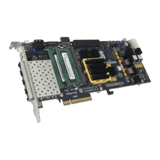
The NetFPGA-SUME board comes with two Micron MT8KTF51264HZ-1G9 4GB DDR3 SDRAM SODIMM, which
employs an 932.84MHz 64bit-wide data bus capable of operating at a data rate of 1866MT/s. Project development
with the SDRAM involves using the Xilinx Memory Interface Generator (MIG) in Vivado Design Suite. The interface
is automatically configured by the MIG for use with the AXI4 system bus and provide a fixed 4:1 memory to bus
clock ratio. The input clock for both SDRAM SODIMMs is a 233MHz clock generated by Discera DSC1103 Low Jitter
Precision LVDS Oscillator. The clock period of SDRAM is configured to 1177ps (849.62MHz), equivalent to
1700MT/s, due to the read margin issues. Please refer to Xilinx
The NetFPGA-SUME uses a VCC
see
Xilinx 7 Series FPGAs Memory Interface Solutions User Guide (UG586)
204-Pin DDR3L SODIMM
datasheet for more details. The DDR3 project in unit test project in netfpga repository
provides a good starting point for project development.
4.2
QDRII+ SRAM
Three Cypress CY7C25652KV18 Quad Data Rate II+ (QDRII+) SRAMs are provided for applications that require high
speed, low latency memory. Each component provides a 36 bit wide data bus and has a density of 72 Megabits.
Common applications include FIFO buffers and look-up tables. The notion of "Quad" data rate comes from the
ability to simultaneously read from a unidirectional read port and write to a unidirectional write port on both clock
edges. The QDRII+ SRAMs on NetFPGA-SUME board are capable of operating at up to 500MHz to yield data
transfer rates of up to 1GT/s per 36-bit wide data bus. The Xilinx Memory Interface Generator (MIG) is able to
generate and configure a native interface into the QDRII+ via the user friendly wizard tool. More information
regarding the QDRII+ memory part and the Xilinx MIG tool can be found in the Cypress
CY7C25632KV18/CY7C25652KV18 datasheet, the Cypress Application Note QDR-II, QDR-II+, DDR-II, DDR-II+ Design
Guide (AN4065), and the Xilinx 7-Series FPGA Memory Interface Solutions User Guide (UG586).
QDRA and QDRB share FPGA bank 17, which means that in order to access them simultaneously, a bank sharing
solution must be used that extends beyond the default functionality of the MIG. This solution is still currently being
developed. Please refer to Xilinx Answer Record 41706 for further information.
5
Storage
5.1
FLASH
Onboard parallel flash is available for storing FPGA bitstreams. For information on writing bitstreams to flash and
configuring the FPGA from stored bitstreams, see the section titled
Copyright Digilent, Inc. All rights reserved.
Other product and company names mentioned may be trademarks of their respective owners.
of 2.0V to support high performance DDR3 frequency settings. Please
AUX-IO
Answer Record AR61853
for further information.
and the micron
1GB, 2GB, 4GB (x64, SR)
"Configuration using Parallel
Flash".
Page 14 of 18
