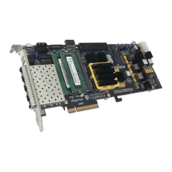
Digilent NetFPGA-SUME Referenzhandbuch - Seite 17
Blättern Sie online oder laden Sie pdf Referenzhandbuch für Hauptplatine Digilent NetFPGA-SUME herunter. Digilent NetFPGA-SUME 20 Seiten.

NetFPGA-SUME™ Reference Manual
Clock Name
Source
IC16 DSC1103,
FPGA_SYSCLK
IC17 SI5330
IC16 DSC1103,
QDRII_SYSCLK
IC17 SI5330
IC16 DSC1103,
QDRIIC_SYSCLK
IC17 SI5330
SATA_SYSCLK
IC21 DSC1103
SFP_CLK
IC20 SI5324
DDR3_SYSCLK
IC18 DSC1103
PCIE-CLK
PCI-E Connector
FMC_GBT_CLK0
FMC Connector
FMC_GBT_CLK1
FMC Connector
FMC_CLK0
FMC Connector
FMC_CLK1
FMC Connector
6
Expansion Interfaces
6.1
FMC
The NetFPGA-SUME board includes a VITA-57 compatible FMC (FPGA Mezzanine Card) carrier connector. A High
Pin Count (HPC) connector is used to provide the maximum possible compatibility with a variety of commercially
available mezzanine cards. Select I/O ports on the XC7V690T are connected to all of the standard Low Pin Count
(LPC) signals on the connector, due to the limitations of the FFG1761 package. All the I/O ports connected to FMC
connector only supports 1.8V logic. All 10 differential send/receive pairs for GTX transceivers are also supported.
Please refer to the American National Standards Institute ANSI/VITA 57.1 FPGA Mezzanine Card (FMC) Standard
for additional details regarding standard FMC module and carrier requirements. Refer to Appendix B of this
document for specific I/O constraints relating FPGA pins to their associated FMC control and connector pins.
6.2
QTH
The NetFPGA-SUME board includes a Samtec 0.5 mm-pitch QSH/QTH family of high-speed board-to-board
communication. The QTH connector wires out 8 transceivers from Virtex-7 FPGAs and tested at a speed of
12.5Gbps. Please refer to
Samtec website
footprint, etc.
6.3
Pmod
The NetFPGA-SUME board also provides a Pmod port for peripheral extension. The Pmod port is arranged as a 2×6
vertical, 100-mil female connector that mates with standard 2×6 pin headers. Each 12-pin Pmod port provides two
Copyright Digilent, Inc. All rights reserved.
Other product and company names mentioned may be trademarks of their respective owners.
Destination
FPGA (H19, G18)
FPGA (AD32, AD33)
FPGA (AU14, AU13)
FPGA
(MGTREFCLK0_116:T8, T7)
FPGA (MGTREFCLK0_118:
E10, E9)
FPGA (E34, E35)
FPGA (MGTREFCLK1_115:
AB8, AB7)
FPGA (MGTREFCLK0_112:
AT8, AT7)
FPGA (MGTREFCLK1_112:
AU10, AU9)
FPGA (AR27, AT27)
FPGA (AV34, AV35)
for additional details regarding the QTH connector's specification,
Frequency
Common Useage
200MHz
General Purpose
Used by MIG for QDRIIA,
200MHz
QDRIIB
200MHz
Used by MIG for QDRIIC
Used by SATA
150MHz
transceivers (Bank 116
Lane 0/1)
156.25MHz
Shared by transceivers
(Configurable)
of SFP+ and QTH
Shared by MIG for
233.33MHz
DDR3A, DDR3B
Used by PCI-Express
100MHz
Core
Used by FMC
-
transceivers (Bank 111,
112, 113)
Used by FMC
-
transceivers (Bank 111,
112, 113)
-
Used by FMC card
-
Used by FMC card
Page 17 of 18
