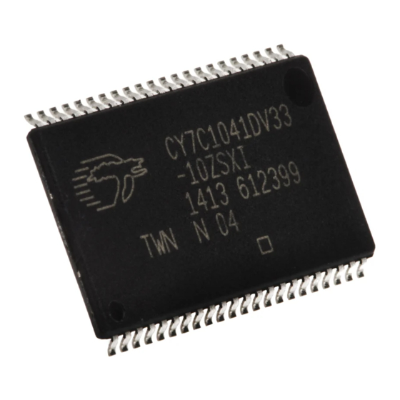
Cypress Semiconductor CY7C1041DV33 Spezifikationsblatt - Seite 6
Blättern Sie online oder laden Sie pdf Spezifikationsblatt für Computer Hardware Cypress Semiconductor CY7C1041DV33 herunter. Cypress Semiconductor CY7C1041DV33 14 Seiten. 4 mbit (256k x 16) static ram

Data Retention Characteristics
Parameter
V
V
for Data Retention
DR
CC
I
Data Retention Current
CCDR
[6]
t
Chip Deselect to Data Retention Time
CDR
[15]
t
Operation Recovery Time
R
Data Retention Waveform
V
CC
CE
Switching Waveforms
ADDRESS
DATA OUT
PREVIOUS DATA VALID
Notes
12. The internal write time of the memory is defined by the overlap of CE LOW and WE LOW. CE and WE must be LOW to initiate a write and the transition of either of
these signals can terminate the write. The input data setup and hold timing should be referenced to the leading edge of the signal that terminates the write.
13. The minimum write cycle time for Write Cycle No. 4 (WE controlled, OE LOW) is the sum of t
14. No input may exceed V
+ 0.3V.
CC
15. Full device operation requires linear V
16. Device is continuously selected. OE, CE, BHE, and BHE = V
17. WE is HIGH for read cycle.
Document #: 38-05473 Rev. *E
Over the Operating Range
Description
V
CC
CE > V
V
IN
3.0V
t
CDR
Figure 4. Read Cycle No. 1
t
AA
t
OHA
> 50 μs or stable at V
ramp from V
to V
CC
DR
CC(min.)
.
IL
[14]
Conditions
= V
= 2.0V,
DR
– 0.3V,
CC
> V
– 0.3V or V
< 0.3V
CC
IN
DATA RETENTION MODE
V
> 2V
DR
[16, 17]
t
RC
and t
.
HZWE
SD
> 50 μs.
CC(min.)
CY7C1041DV33
Min
Max
2.0
Ind'l
10
Auto
15
0
t
RC
3.0V
t
R
DATA VALID
Page 6 of 13
Unit
V
mA
mA
ns
ns
[+] Feedback
[+] Feedback
