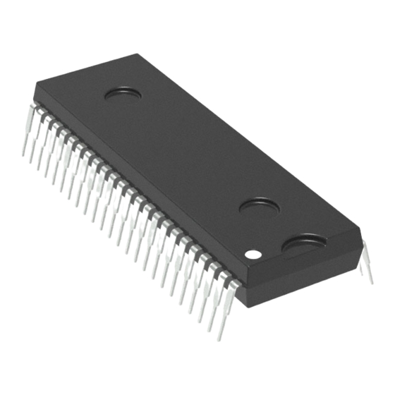
Cypress Semiconductor CY7C131A Spezifikationsblatt
Blättern Sie online oder laden Sie pdf Spezifikationsblatt für Computer Hardware Cypress Semiconductor CY7C131A herunter. Cypress Semiconductor CY7C131A 20 Seiten. 1k x 8 dual-port static ram

Features
■
True dual-ported memory cells, which allow simultaneous
reads of the same memory location
■
1K x 8 organization
■
0.65 micron CMOS for optimum speed and power
■
High speed access: 15 ns
■
Low operating power: I
= 110 mA (maximum)
CC
■
Fully asynchronous operation
■
Automatic power down
■
Master CY7C130/130A/CY7C131/131A easily expands data
bus width to 16 or more bits using slave CY7C140/CY7C141
■
BUSY output flag on CY7C130/130A/CY7C131/131A; BUSY
input on CY7C140/CY7C141
■
INT flag for port-to-port communication
■
Available in 48-pin DIP (CY7C130/130A/140), 52-pin PLCC,
52-pin TQFP
■
Pb-free packages available
Logic Block Diagram
R/W
CE
OE
I/O
I/O
BUSY
L
A
A
INT
L
Notes
1. CY7C130 and CY7C130A are functionally identical; CY7C131 and CY7C131A are functionally identical.
2. CY7C130/130A/CY7C131/131A (Master): BUSY is open drain output and requires pull-up resistor.
CY7C140/CY7C141 (Slave): BUSY is input.
3. Open drain outputs: pull-up resistor required.
Cypress Semiconductor Corporation
Document #: 38-06002 Rev. *E
L
L
L
7L
I/O
CONTROL
0L
[2]
9L
ADDRESS
DECODER
0L
CE
L
OE
L
R/W
L
[3]
•
198 Champion Court
1K x 8 Dual-Port Static RAM
Functional Description
The CY7C130/130A/CY7C131/131A/CY7C140
are high speed CMOS 1K by 8 dual-port static RAMs. Two ports
are provided permitting independent access to any location in
memory. The CY7C130/130A/ CY7C131/131A can be used as
either a standalone 8-bit dual-port static RAM or as a master
dual-port RAM in conjunction with the CY7C140/CY7C141 slave
dual-port device in systems requiring 16-bit or greater word
widths. It is the solution to applications requiring shared or
buffered data, such as cache memory for DSP, bit-slice, or multi-
processor designs.
Each port has independent control pins; chip enable (CE), write
enable (R/W), and output enable (OE). Two flags are provided
on each port, BUSY and INT. BUSY signals that the port is trying
to access the same location currently being accessed by the
other port. INT is an interrupt flag indicating that data is placed
in a unique location (3FF for the left port and 3FE for the right
port). An automatic power down feature is controlled indepen-
dently on each port by the chip enable (CE) pins.
The CY7C130/130A and CY7C140 are available in 48-pin DIP.
The CY7C131/131A and CY7C141 are available in 52-pin
PLCC, 52-pin Pb-free PLCC, 52-pin PQFP, and 52-pin Pb-free
PQFP.
I/O
CONTROL
MEMORY
ADDRESS
ARRAY
DECODER
ARBITRATION
LOGIC
(7C130/7C131 ONLY)
CE
R
AND
INTERRUPT LOGIC
OE
R
R/W
R
•
San Jose
CY7C130, CY7C130A
CY7C131, CY7C131A
CY7C140, CY7C141
[1]
and CY7C141
R/W
R
CE
R
OE
R
I/O
7R
I/O
0R
BUSY
R
A
9R
A
0R
[3]
INT
R
,
CA 95134-1709
•
408-943-2600
Revised December 09, 2008
[+] Feedback
