Cypress Semiconductor CY7C68023 Spezifikationsblatt - Seite 6
Blättern Sie online oder laden Sie pdf Spezifikationsblatt für Computer Hardware Cypress Semiconductor CY7C68023 herunter. Cypress Semiconductor CY7C68023 9 Seiten. Ez-usb nx2lp usb 2.0 nand flash controller

Table 6-1. Variable Configuration Data And Default ROM Values
Configuration Data
Vendor ID
Product ID
Serial Number
Manufacturer String
Product String
Enable Write Protection
SCSI Device Name
7.0
Design Notes For The Quad Flat No Lead
(QFN) Package
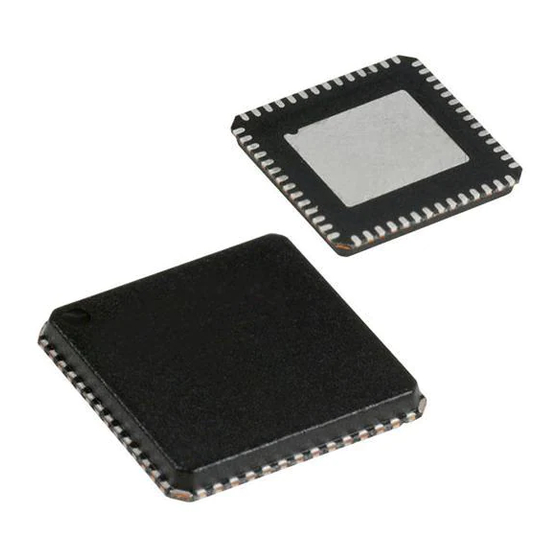
The NX2LP comes in a 56-pin QFN package, which utilizes a
metal pad on the bottom to aid in heat dissipation. The low-
power operation of the NX2LP makes the thermal pad on the
bottom of the QFN package unnecessary. Because of this,
PCB layout may utilize the space under the NX2LP for routing
signals as needed, provided that any traces or vias under the
thermal pad are covered by solder mask or other material to
prevent shorting. Standard PCB layout recommendations for
USB devices still apply.
For further information on this package design, please refer to
the application note from AMKOR titled "Surface Mount
Assembly of AMKOR's MicroLeadFrame (MLF) Technology."
This application note provides detailed information on board
mounting guidelines, soldering flow, rework process, etc.
8.0
PCB Layout Recommendations
The following recommendations should be followed to ensure
reliable High-speed USB performance operation.
• A four-layer impedance controlled board is recommended
to ensure best signal quality.
• Specify impedance targets (ask your board vendor what
they can achieve).
• Maintain trace widths and trace spacing to control imped-
ance.
• Minimize stubs on DPLUS and DMINUS to avoid reflected
signals.
• Place any connections between the USB connector shell
and signal ground near the USB connector.
• Use bypass/flyback caps on VBUS, placed near connector.
• Keep DPLUS and DMINUS trace lengths to within 2 mm of
each other in length, with preferred length of 20–30 mm.
Note:
2.
If an alternate clock source is input on XTALIN, it must be supplied with standard 3.3V signaling characteristics and XTALOUT must be left floating.
Document #: 38-08055 Rev. *B
Description
USB Vendor ID (Assigned by USB-IF)
USB Product ID (Assigned by designer)
USB serial number
Manufacturer string in USB descriptors
Product string in USB descriptors
Enables write protection capability
String shown in the device manager properties
CY7C68023/CY7C68024
• Maintain a solid ground plane under the DPLUS and DMI-
NUS traces. Do not allow the plane to be split under these
traces.
• Place no vias on the DPLUS or DMINUS trace routing.
• Isolate the DPLUS and DMINUS traces from all other signal
traces (use >10 mm. spacing for best signal quality).
Source for recommendations:
• EZ-USB FX2 PCB Design Recommendations,
press.com/cfuploads/support/app_notes/FX2_PCB.pdf.
• High-speed USB Platform Design Guidelines,
www.usb.org/developers/data/hs_usb_pdg_r1_0.pdf.
9.0
Absolute Maximum Ratings
Storage Temperature ...................................–65°C to +150°C
Ambient Temperature with Power
Supplied............................................................ 0°C to +70°C
Supply Voltage to Ground Potential................–0.5V to +4.0V
DC Input Voltage to Any Input Pin ................................ 5.25V
DC Voltage Applied to Outputs
in High-Z State..................................... –0.5V to VCC + 0.5V
Power Dissipation..................................................... 300 mW
Static Discharge Voltage.............................................. 2000V
Max Output Current per IO port................................... 10 mA
10.0
Operating Conditions
T
(Ambient Temperature Under Bias) ............. 0°C to +70°C
A
Supply Voltage............................................+3.00V to +3.60V
Ground Voltage.................................................................. 0V
F
(Oscillator or Crystal Frequency) ... 24 MHz ± 100 ppm
OSC
Default ROM Value
0x04B4 (Cypress)
0x6813
N/A
N/A
N/A
Enabled
N/A
www.cy-
[2]
Parallel Resonant
Page 6 of 9
[+] Feedback
