ATX Q series Manuel d'installation et d'utilisation - Page 5
Parcourez en ligne ou téléchargez le pdf Manuel d'installation et d'utilisation pour {nom_de_la_catégorie} ATX Q series. ATX Q series 18 pages. Qpair redundancy switch amplifier system

DESCRIPTION OF INTERFACES
1.
Description of Interfaces
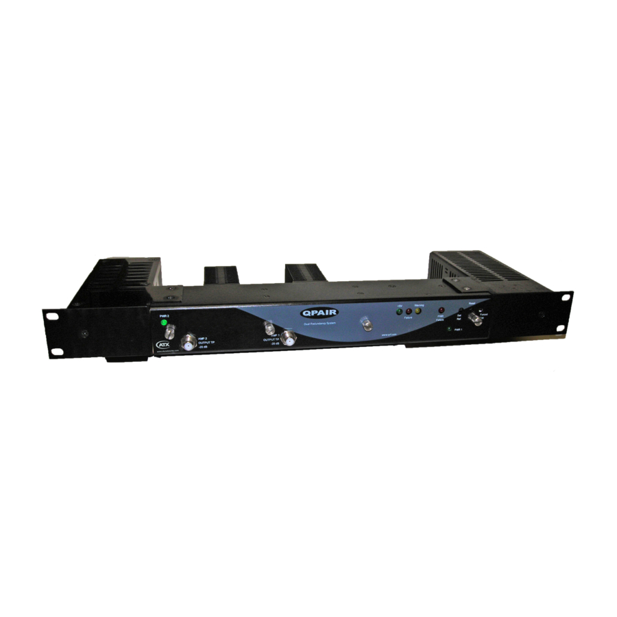
The QPAIR system (the system) has fi ve sections: two modular amplifi er sections, the RF switch section and two replaceable
power supplies.
Replaceable Power Supplies:
AC Input (100-240 VAC, 50 or 60 Hz) or -48 VDC input.
The system can also be ordered with (1) AC input and (1) 48 VDC input for source redundancy.
The power supply confi guration depends on user specifi cation at time of ordering.
Description: Both of the power supplies are connected at the same time via their designated terminals. In normal operation,
the power supplies are in redundant mode with no switching required. Power supply 1 and power supply 2 each have a green
LED (PWR 1 and PWR 2) on the front to indicate normal power supply operation. The PWR Failure red LED (see Figure 1) on
the front also indicates power supply status. If the PWR Failure LED is solid red, then that indicates the PWR1 supply is not
operational and if the LED is blinking, then that indicates the PWR 2 supply is not operational. This may also be noted during
the installation when only one power supply is initially plugged into source voltage. The PWR Failure LED will either be solid or
blink depending on which power supply is connected to source power fi rst. The PWR Failure LED will remain lit after any PS
failure or source power failure. Failure is also detected upon unplugging either power supply from the power source. Anytime
the PWR failure LED is lit and voltage has been restored, or immediately after installation, the RESET button must be pushed
to activate normal operation.
RF Amplifi er Connections:
a)
Rear of Chassis: this section only describes the amplifi er connections, not the switch connections.
Input to AMP 1 (labeled RF IN and located immediately at the lower left of the left heat sink).
Output from AMP 1 (labeled RF OUT and located at the upper right of the left heat sink).
Input to AMP 2 (labeled RF IN and located immediately at the lower left of the right heat sink).
Output from AMP 2 (labeled RF OUT and located at the upper right of the right heat sink).
b)
Front of Chassis: (with cover removed):
RF test point (-20 dB) located at left front of each amplifi er module and labeled "AMP1 OUTPUT TP" on AMP 1 and
"AMP2 OUTPUT TP" on AMP 2. A Pad socket for input level and pad socket for output level adjustment is located in
each amplifi er compartment. The equalizer socket for input level and equalizer socket for output level adjustment are
also located in each amplifi er compartment.
Description: The primary and the secondary amplifi er are identical. However, this system designates AMP 1 as the primary
amplifi er and AMP 2 is designated as the secondary amplifi er. When we discuss the term primary amplifi er, we are discussing
AMP 1 and when we use the term secondary amplifi er, we are discussing AMP 2. The primary amplifi er is located approximately
at the middle of the chassis and the secondary amplifi er is located toward the left side of the chassis from a front view. Each
Q-Series
Amplifi ers – QPAIR Redundant Amplifi er System – Installation & Operation Manual
®
QPAIR Redundant Amplifi er System Front View
QPAIR Redundant Amplifi er System Rear View
(one located at each end of the chassis)
(Rear View)
CHAPTER 1: DESCRIPTION OF INTERFACES
1-1
