Alinx ALTER AC4040 Manuel de l'utilisateur - Page 6
Parcourez en ligne ou téléchargez le pdf Manuel de l'utilisateur pour {nom_de_la_catégorie} Alinx ALTER AC4040. Alinx ALTER AC4040 20 pages. Core board
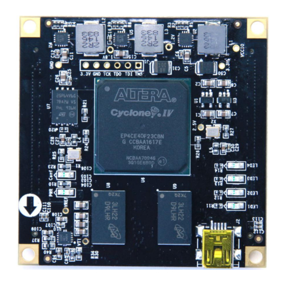
Further, in order to allow DDR2 work properly, it is necessary to provide a
reference voltage VREF and the termination voltage VTT is DDR2 DDR2 chip
address lines and control lines, and VTT voltage VREF are 0.9V. Figure 3-2-1
detailed the power supply schematic below:
Figure 2-3: DDR2 Power Circuit on the Core Board
DDR2 connected to the BANK3 and BANK4 of the FPGA.
DDR2 Pin Assignment
Pin Name
DDR2_A[0]
6 / 20
ALINX ALTERA Core Board AC4040 User Manual
Figure 2-2: DDR2 Power for VTT/VREF
FPGA Pin
U10
Amazon Store: https://www.amazon.com/alinx
Pin Name
DDR2_A[11]
FPGA Pin
AB3