Alinx ALTER AC4075 Manuel de l'utilisateur - Page 5
Parcourez en ligne ou téléchargez le pdf Manuel de l'utilisateur pour {nom_de_la_catégorie} Alinx ALTER AC4075. Alinx ALTER AC4075 19 pages. Core board

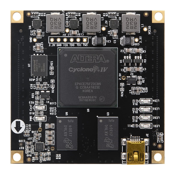
FPGA+ 2DDR2 core board is based on ALTERA
EP4CE75F23C8. This chip develops a high-performance core board with high
speed, high bandwidth and high capacity. It is suitable for video image
processing and high-speed data acquisition.
This core board uses two pieces of MICRON's MT47H64M16HR-3IT
DDR2 chip with a total capacity of 2Gbit; two DDR2s form a 32-bit bus mode,
and the read/write data bandwidth between FPGA and DDR2 is up to 8.5Gb;
this configuration can satisfy 4 channels of 1080p video processing needs.
This core board extends 168 IO ports (73 pairs of LVDS differential), which
is a good choice for users who need a lot of IO. Moreover, the FPGA chip to the
interface is treated with the same length, and the core board size is only 60*60
(mm), which is very suitable for secondary development.
Part 2: DDR2 DRAM
Figure 2-1 detailed part of the DDR2 schematic (For details, please refer to
the schematic provided by us.)
Further, in order to allow DDR2 work properly, it is necessary to provide a
reference voltage VREF and the termination voltage VTT is DDR2 DDR2 chip
5 / 19
ALINX ALTERA Core Board AC4075 User Manual
Figure 2-1: DDR2 schematic
Amazon Store: https://www.amazon.com/alinx
CYCLONE IV series
