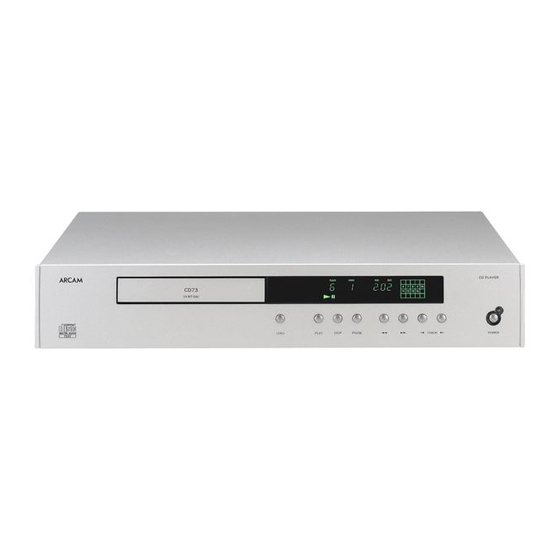
Arcam DiVA CD73 Manuel d'entretien - Page 3
Parcourez en ligne ou téléchargez le pdf Manuel d'entretien pour {nom_de_la_catégorie} Arcam DiVA CD73. Arcam DiVA CD73 13 pages. Compact disc player

Analogue power supplies – Standby control
The Analogue audio supply is under relay control and
has over-current protection on both + and – phases,
this is provided by FS503 and FS504 the output sides
of these fuses drive into bridge rectifier BR502, this
bridge rectifier package intern supplies the
unregulated +/- 18v D.C rails (these are used to
drive an optional DAC board).
The +/- 18v unregulated D.C rails are regulated by
U504 (+) and U505 (-) and provide the +/- 12V(A)
supplies.
We use the unregulated +18v to create the clean
+5(A) supply using regulator U506, this supply is fed
to the DAC card option socket at location SK203 but
within the CD73 this supply becomes known as the
+5(DAC) on the audio stage circuit diagram and is
used to power the DAC chip only.
The Relay at location RLY501 switches the low
voltage A.C from the secondary to the bridge rectifier
at location BR502 we will also see that relay RLY502
switches the F1 and F2 rails to the display filament,
both if these relays are switched on/off by the control
line seen as STANDBY on the circuit diagrams.
When in the on state we should see -4.8V D.C with
respect to DGND on the Base of Q309.
Clock generation.
The clock circuit is based around the 16.9344MHz
crystal at location X401 the clock from the crystal is
amplified by transistor Q403 before being dived into
two separate clock streams by the 74HCUO4 buffer
at location U402a/b/c/d, the output of U402c is fed to
the DAC (U401) and the output of U402d forms the
master clock for the DSP at location U201.
The third clock within the circuit (4MHz) can be found
at location X701A and is used to drive the Display –
Control – Keyboard scan chip U701.
Fig 2. Laser diode direct monitor points
Mechanism and Micro engine.
Three chips have direct control over the
Mechanism their locations and primary functions
follow.
U201 CXD3017Q DSP
o 16k onboard RAM error correction
o Sub Q error data error detection
o CPU interface – U701 display board
o CD text demodulator
o Auto gain for Servo loop
o Focus bias adjustment
o CPU interface
o Direct interface to DAC
U101 CXA2581N
o RF AC-DC summing
o Focus error amplifier
o Tracking error amplifier
o Centre error amplifier
U202 BA6392FP
o 4 channel BTL driver
o Direct turntable motor control (CH 4)
o Focus coil drive +/- (CH2)
o Focus coil drive +/- (CH3)
o Laser sledge drive (CH1)
We can simplify the circuit if we look at the signal
path from the Laser optic this can be seen as
laser optic output amplifier U101 – DSP control
micro U201 – Laser tracking, Focus, Spindle,
Sled control BTL U202.
The CXA2581N at location U101 is fed 6 lines of
R.F output from the laser optic these can be seen
as inputs A – F on pins 6 – 11, the inputs on pins
10 and 11 are labelled E and F these are used
the internal tracking error summing this signal is
then seen as a VC output on pin 27.
We can directly monitor the R.F output from the
Laser Photo diodes at location shown in Fig 2.
These can be seen as the focus outputs on
resistors R103 and R104 these appear above the
letters e and f on the diagram, between the two
resistors the Laser diode outputs can be seen on
the solder feed thru points labelled as a, b, c, d.
