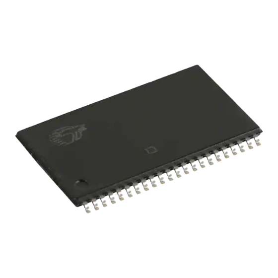
Cypress Semiconductor CY62147EV30 MoBL Manuel
Parcourez en ligne ou téléchargez le pdf Manuel pour {nom_de_la_catégorie} Cypress Semiconductor CY62147EV30 MoBL. Cypress Semiconductor CY62147EV30 MoBL 14 pages. 4-mbit (256k x 16) static ram

Features
■
Very high speed: 45 ns
■
Temperature ranges
❐
Industrial: –40°C to +85°C
❐
Automotive-A: –40°C to +85°C
❐
Automotive-E: –40°C to +125°C
■
Wide voltage range: 2.20V to 3.60V
■
Pin compatible with CY62147DV30
■
Ultra low standby power
Typical standby current: 1 μA
❐
Maximum standby current: 7 μA (Industrial)
❐
■
Ultra low active power
❐
Typical active current: 2 mA at f = 1 MHz
■
Easy memory expansion with CE
■
Automatic power down when deselected
■
CMOS for optimum speed and power
■
Available in Pb-free 48-ball VFBGA (single/dual CE option) and
44-pin TSOPII packages
■
Byte power down feature
Functional Description
The CY62147EV30 is a high performance CMOS static RAM
organized as 256K words by 16 bits. This device features
advanced circuit design to provide ultra low active current. It is
Logic Block Diagram
POWER DOWN
Note
1. BGA packaged device is offered in single CE and dual CE options. In this data sheet, for a dual CE device, CE refers to the internal logical combination of CE
CE
such that when CE
is LOW and CE
2
1
Cypress Semiconductor Corporation
Document #: 38-05440 Rev. *G
[1]
and OE features
A
10
A
9
A
8
A
7
A
6
A
5
A
4
A
3
A
2
A
1
A
0
CE
BHE
CIRCUIT
BLE
is HIGH, CE is LOW. For all other cases CE is HIGH.
2
•
198 Champion Court
4-Mbit (256K x 16) Static RAM
ideal for providing More Battery Life™ (MoBL
cations such as cellular telephones. The device also has an
automatic power down feature that significantly reduces power
consumption when addresses are not toggling. Placing the
device into standby mode reduces power consumption by more
than 99% when deselected (CE HIGH or both BLE and BHE are
HIGH). The input and output pins (IO
in a high impedance state when:
■
Deselected (CE HIGH)
■
Outputs are disabled (OE HIGH)
■
Both Byte High Enable and Byte Low Enable are disabled
(BHE, BLE HIGH)
■
Write operation is active (CE LOW and WE LOW)
To write to the device, take Chip Enable (CE) and Write Enable
(WE) inputs LOW. If Byte Low Enable (BLE) is LOW, then data
from IO pins (IO
through IO
0
specified on the address pins (A
Enable (BHE) is LOW, then data from IO pins (IO
is written into the location specified on the address pins (A
through A
).
17
To read from the device, take Chip Enable (CE) and Output
Enable (OE) LOW while forcing the Write Enable (WE) HIGH. If
Byte Low Enable (BLE) is LOW, then data from the memory
location specified by the address pins appear on IO
Byte High Enable (BHE) is LOW, then data from memory
appears on IO
to IO
8
complete description of read and write modes.
For best practice recommendations, refer to the Cypress
application note
AN1064, SRAM System
DATA IN DRIVERS
256K x 16
RAM Array
COLUMN DECODER
,
•
San Jose
CY62147EV30 MoBL
®
) in portable appli-
through IO
0
15
) is written into the location
7
through A
). If Byte High
0
17
through IO
8
. See the
Truth Table
on page 9 for a
15
Guidelines.
IO
–IO
0
7
IO
–IO
8
15
BHE
WE
[1]
CE
OE
BLE
CA 95134-1709
•
408-943-2600
Revised March 31, 2009
®
) are placed
)
15
0
to IO
. If
0
7
and
1
[+] Feedback
