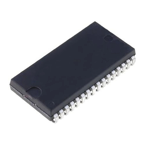
Cypress Semiconductor CY7C1018DV33 Fiche technique - Page 3
Parcourez en ligne ou téléchargez le pdf Fiche technique pour {nom_de_la_catégorie} Cypress Semiconductor CY7C1018DV33. Cypress Semiconductor CY7C1018DV33 9 pages. 1-mbit (128k x 8) static ram

[3]
Capacitance
Parameter
Description
C
Input Capacitance
IN
C
Output Capacitance
OUT
[3]
Thermal Resistance
Parameter
Description
Θ
Thermal Resistance
JA
(Junction to Ambient)
Θ
Thermal Resistance
JC
(Junction to Case)
AC Test Loads and Waveforms
Z = 50Ω
OUTPUT
* CAPACITIVE LOAD CONSISTS
OF ALL COMPONENTS OF THE
TEST ENVIRONMENT
Notes
3. Tested initially and after any design or process changes that may affect these parameters.
4. AC characteristics (except High-Z) are tested using the load conditions shown in Figure (a). High-Z characteristics are tested for all speeds using the test load
shown in Figure (c).
Document #: 38-05465 Rev. *D
Test Conditions
T
= 25°C, f = 1 MHz, V
A
Test Conditions
Still Air, soldered on a 3 × 4.5 inch,
four-layer printed circuit board
[4]
50 Ω
30 pF*
1.5V
(a)
High-Z characteristics:
3.3V
OUTPUT
5 pF
(c)
= 3.3V
CC
Wide SOJ
ALL INPUT PULSES
3.0V
90%
10%
GND
Rise Time: 1 V/ns
R 317Ω
R2
351Ω
CY7C1018DV33
Max.
Unit
8
pF
8
pF
400-Mil
Unit
°C/W
57.61
°C/W
40.53
90%
10%
Fall Time: 1 V/ns
(b)
Page 3 of 9
[+] Feedback
