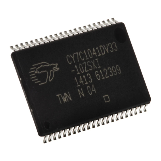
Cypress Semiconductor CY7C1041DV33 Fiche technique - Page 8
Parcourez en ligne ou téléchargez le pdf Fiche technique pour {nom_de_la_catégorie} Cypress Semiconductor CY7C1041DV33. Cypress Semiconductor CY7C1041DV33 14 pages. 4 mbit (256k x 16) static ram

Switching Waveforms
ADDRESS
BHE, BLE
WE
CE
DATAIO
Figure 8. Write Cycle No. 3 (WE Controlled, OE HIGH During Write)
ADDRESS
CE
WE
OE
BHE, BLE
DATA IO
NOTE 21
Note
21. During this period the IOs are in the output state and input signals should not be applied.
Document #: 38-05473 Rev. *E
(continued)
Figure 7. Write Cycle No. 2 (BLE or BHE Controlled)
t
SA
t
AW
t
SCE
t
AW
t
SA
t
HZOE
t
WC
t
BW
t
PWE
t
SCE
t
SD
t
WC
t
PWE
t
SD
DATA
VALID
IN
CY7C1041DV33
t
HA
t
HD
[19, 20]
t
HA
t
HD
Page 8 of 13
[+] Feedback
[+] Feedback
