DAQ system UVC-FRM01 Panduan Pengguna - Halaman 7
Jelajahi secara online atau unduh pdf Panduan Pengguna untuk Motherboard DAQ system UVC-FRM01. DAQ system UVC-FRM01 14 halaman.
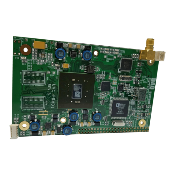
3.3 Connector Pin-out
The following describes the connector used in UVC-FRM01.
3.3.1 CN1 Connector
This is an external HD-SDI signal line connector.
3.3.2 J1 Connector
It is a 5V external DC power connector.
3.3.3 J4 Connecter
J4 is a JTAG (Joint Test Action Group) connector that is used to update the FPGA
program of the board. It is not normally used when operating the board.
3.3.4 J6 Connecter
The figure below shows the pin map of the external input/output J5 connector of the
board.
1
3
5
7
2
4
6
[Table 1. J5 Connector Description]
No.
1
2
3
4
5
6
7
8
9
10
11
12
9
11
13
15
17
19
21
8
10
12
14
16
18
20
22
[Figure 3-2. J5 Connector (Top View)]
Name
N.C
Not Connect
Not Connect
N.C
Not Connect
N.C
N.C
Not Connect
+5V
+5V Power
+5V
+5V Power
+5V
+5V Power
+5V Power
+5V
Not Connect
N.C
GND
Ground
N.C
Not Connect
N.C
Not Connect
23
25 27
29
31
33
35
37
26
28
30
32
34
36
24
Description
7-
-
UVC-FRM01 Users Manual (Rev 1.0)
51
39
41
43
45
47
49
38
40
42
44
46
48
50
Remark
http://www.daqsystem.com