Broadcom ACPL-352J Panduan Referensi - Halaman 9
Jelajahi secara online atau unduh pdf Panduan Referensi untuk Motherboard Broadcom ACPL-352J. Broadcom ACPL-352J 15 halaman. Vincotech h6.5 3-level igbt flowpack module evaluation board
ACPL-352J Reference Manual
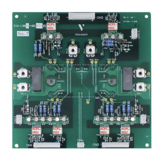
Vincotech H6.5 3-Level IGBT flowPACK Module Evaluation Board
Figure 8: Simulation of the Operating Waveform
2.3 Gate Drive Design
Figure 9: ACPL-352J Gate Drive Circuit
The schematic shows the gate drive design for IGBT, T12 of the H6.5 module.
The ACPL-352J has a LED input control input and three fault reporting mechanisms: namely V
under voltage lockout
DD2
(UVLO), IGBT over current (FAULT) and IGBT gate status (GFAULT). These open drain FAULT, UVLO and GFAULT outputs
are connected to 10-kΩ pull-up resistors (R1/R3) and 1nF filtering capacitors (C1/C2) and are suitable for wired OR
applications. UVLO has the highest fault priority and follows by FAULT and GFAULT (GFAULT is not used in this evaluation
board).
The supplies (V
and V
) are connected to 1 µF (C3) and pairs of 10 µF/0.1 µF (C9/C10, C11/C12, C14/C15) bypass
DD1
DD2
decoupling capacitors to provide the large transient currents necessary during a switching transition.
The two resistors (R5/R6) connected to input LED's anode and cathode are recommended to be split in the ratio of 3:1. They
will help to balance the common mode impedances at the LED's anode and cathode. This helps to equalize the common
mode voltage changes at the anode and cathode to give high CMR performance of more than100 kV/µs.
The OC pin of ACPL-352J is connected to the collector of IGBT T12 via a high voltage blocking diode, D5 and resistor R13.
Zener diode, D15 is used to adjust the threshold voltage of over current detection. Blanking capacitor, C12 is used prevent
false fault detection by filtering high frequency noise transient.
Broadcom Confidential
ACPL-352J-Ref-RM100
9