Alinx AN8238 Panduan Pengguna - Halaman 12
Jelajahi secara online atau unduh pdf Panduan Pengguna untuk Unit Kontrol Alinx AN8238. Alinx AN8238 17 halaman. 2-channel high speed ad module
2-Channel High Speed AD Module AN9238 User Manual
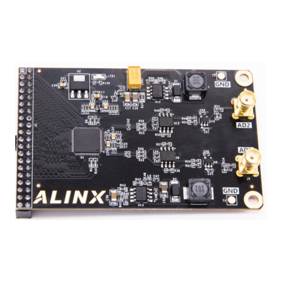
Part 4: Hardware Connection and Testing
The
hardware
development board is very simple, just plug the 40-pin interface with the
expansion port of the development board (AX301B/AX4010 connect to J1 port,
AX309 connect to J3). The following is the hardware connection diagram of
ALINX AX301B FPGA development board and AN9328:
The FPGA development board is powered on, and the signal generator
generates a positive wave of -5V~+5V with a frequency of 200Khz.
12/17
connection
between AN9328
module
and
FPGA
www.alinx.com