DFI BT9A3 Series Panduan Pengguna - Halaman 19
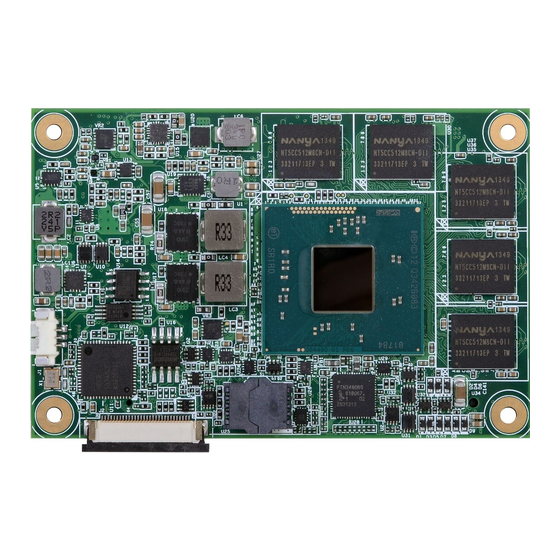
Jelajahi secara online atau unduh pdf Panduan Pengguna untuk Perangkat Keras Komputer DFI BT9A3 Series. DFI BT9A3 Series 19 halaman. Com express mini
GPIO Signals Descriptions
Signal
Pin#
GPO0
A93
GPO1
B54
GPO2
B57
GPO3
B63
GPI0
A54
GPI1
A63
GPI2
A67
GPI3
A85
Power and GND Signal Descriptions
Signal
Pin#
A104~A109
VCC_12V
B104~B109
VCC_5V_SBY
B84~B87
VCC_RTC
A47
A1, A11, A21, A31, A41,
A51, A57, A60, A66, A70,
A80, A90, A100, A110, B1,
GND
B11, B21 ,B31, B41, B51,
B60, B70, B80, B90, B100,
B110
Chapter 3 Hardware Installation
Chapter 3
Pin Type
Pwr Rail /Tolerance
BT9A3 Series
O CMOS
3.3V / 3.3V
PU 100K to 3.3V
PU 100K to 3.3V
I CMOS
PU 100K to 3V3
PU 100K to 3.3V
PU 100K to 3.3V
Pin Type
Pwr Rail /Tolerance
BT9A3 Series
Power
4.75V – 20.0V
4.75V – 20.0V
Power
4.75V - 5.25V
4.75V - 5.25V
Power
2.0V - 3.3V
2.0V - 3.3V
Power
Carrier Board
Description
General purpose output pins.
General purpose input pins.
Carrier Board
Description
Primary power input: +12V nominal. All available VCC_12V pins on the connector(s) shall be used.
The module supplies a wide range of power from 4.75V to 20.0V.
Standby power input: +5.0V nominal. If VCC5_SBY is used, all
available VCC_5V_SBY pins on the connector(s) shall be used. Only
used for standby and suspend functions. May be left unconnected if
these functions are not used in the system design.
Real-time clock circuit-power input. Nominally +3.0V.
Ground - DC power and signal and AC signal return path.
All available GND connector pins shall be used and tied to Carrier
Board GND plane.
19
www.dfi .com