EPC EPC9030 Panduan Memulai Cepat - Halaman 3
Jelajahi secara online atau unduh pdf Panduan Memulai Cepat untuk Motherboard EPC EPC9030. EPC EPC9030 7 halaman. Epc9022, half bridge with gate drive for epc8000 family
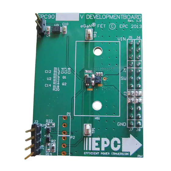
Quick Start Procedure
The development board is easy to set up to evaluate the performance of the eGaN FET. Refer to Figure 2 for proper connect and measurement
setup and follow the procedure below:
1. With power off, connect the input power supply bus to +V
2. With power off, connect the switch node of the half bridge OUT (J3, J4) to your circuit as required.
3. With power off, connect the gate drive input to +V
4. With power off, connect the input PWM control signal to PWM (J2, Pin-1) and ground return to any of the remaining J2 pins.
5. Turn on the gate drive supply – make sure the supply is between 7 V and 12 V range.
6. Turn on the bus voltage to the required value (do not exceed the absolute maximum voltage on V
a. EPC9022, 65 V
b. EPC9023, 100 V
c. EPC9024, 40 V
7. Turn on the controller / PWM input source and probe switching node to see switching operation.
8. Once operational, adjust the bus voltage and load PWM control within the operating range and observe the output switching behavior,
efficiency and other parameters.
9. For shutdown, please follow steps in reverse.
NOTE. When measuring the high frequency content switch node (OUT), care must be taken to avoid long ground leads. Measure the switch node (OUT) by placing the oscilloscope
probe tip through the large via on the switch node (designed for this purpose) and grounding the probe directly across the GND terminals provided. See Figure 3 for proper scope
probe technique.
THERMAL CONSIDERATIONS
The development board showcases the EPC8000 family of eGaN FET. Although the electrical performance surpasses that for traditional silicon
devices, their relatively smaller size does magnify the thermal management requirements. The development board is intended for bench evaluation
with low ambient temperature and convection cooling. The addition of heat-sinking and forced air cooling can significantly increase the current rat-
ing of these devices, but care must be taken to not exceed the absolute maximum die temperature of 125°C.
NOTE. The development board does not have any current or thermal protection on board.
(J5, J6) and ground / return to –VIN (J7, J8).
IN
(J1, Pin-1) and ground return to –V
DD
d. EPC9025, 65 V
e. EPC9027, 40 V
f. EPC9028, 40 V
(J1, Pin-2).
DD
as indicated in the table below:
OUT
g. EPC9029, 65 V
h. EPC9030, 100 V