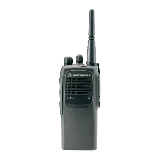
Motorola GP140 Series Informasi Layanan - Halaman 8
Jelajahi secara online atau unduh pdf Informasi Layanan untuk Radio Dua Arah Motorola GP140 Series. Motorola GP140 Series 30 halaman. Professional radio, power distribution and controller
Juga untuk Motorola GP140 Series: Panduan Pengguna (20 halaman), Informasi Layanan (32 halaman), Informasi Layanan (30 halaman), Panduan Servis Dasar (46 halaman)

1-4
A MOSFET Q416 switches in the LiO supply when Vdd is removed. Q416 also provides isolation
from BOOT_CTRL function in the event of radio program flashing. The 3.3V regulator charges the
Lithium battery.
3.4
ModB/Vstby Supply
The supply to the ModB/Vstby pin varies depending on the conditions listed in Table 1-2.
Radio On
Radio Off
Primary battery removed
Flash Mode
3.5
Audio/Signalling Architecture
( Refer to Figure 1-2 and the ASFIC/ON_OFF and Audio Power Amplifier schematic diagrams )
The audio/signalling/filter/companding IC (ASFIC_CMP) and the audio power amplifier, shown in
Figure 1-2, form the main components of the audio/signalling architecture section of the controller
board. Inputs include a 16.8 MHz clock from the synthesizer, recovered audio and squelch, MCU
control signals, and external or internal microphones. Outputs include a microprocessor clock (uP),
modulator output to the synthesizer, and amplified audio signals to an internal or external speaker.
Table 1-2 ModB/Vstby Supply Modes
Condition
Circuit Operation
Vdd supply voltage via CR411
• Vdd turned off
• Q416 gate pulled low by R462
• Q416 switched on
• U410 supplies 3.2V to ModB/Vstby
• Vdd turned off
• Q416 gate pulled low by R462
• Q416 switched on
• Lithium battery provides 3.2V to ModB/Vstby
• Boot_Ctrl line pulled low
• ModA & ModB go low
• Processor in boot-strap mode
THEORY OF OPERATION
