Gan Systems GS-EVB-HBDB-IMS Manuale tecnico - Pagina 9
Sfoglia online o scarica il pdf Manuale tecnico per Scheda madre Gan Systems GS-EVB-HBDB-IMS. Gan Systems GS-EVB-HBDB-IMS 20. 650 v universal half bridge isolated driver motherboard for ims2 & ims3
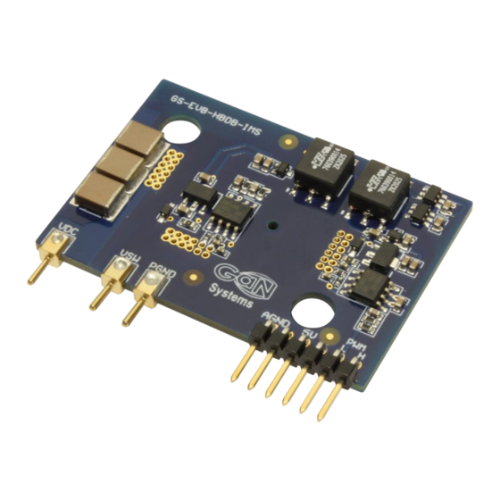
GS-EVB-HBDB-IMS
650 V Universal Half Bridge Isolated Driver Motherboard for IMS2
& IMS3
Technical Manual
____________________________________________________________________________________________________________________________________________
The gate driver circuit on the IMS driver motherboard is powered from a 5V DC source, through the 5V
connector pin. The PWM signals of both GaN devices come from the external PWM, also through the PWM
connector pin. The deadtime of PWM signals is required and should be provided from an external source.
2.4 Temperature Monitoring Hole
A hole is located on the center of the low-side GaN E-mode to assist with the temperature monitoring
during operation. A thermal camera can be used to monitor the case temperature through the temperature
monitoring hole. The temperature measured at the center of GaN
® package will be close to the T
.
PX
J
NOTE: Thermal performance of the transistors is dependent on a number of factors including circuit
configuration, ambient temperature, airflow, and heatsinking. The user is responsible for monitoring the
temperature of the devices to ensure operation remains within specification.
2.5 Installation of IMS Half-Bridge Daughter power board
To achieve the lowest power loop parasitics, it is suggested to solder the IMS half-bridge daughter power
board to the IMS EVB driver motherboard. When soldering by hand, it is important to avoid accidental
short circuits caused by unwanted solder connection between the device gate and source, as shown in
figure 7.
Figure 7 Soldering pin guide
2.6 DC Link Decoupling Capacitors
As it is challenging to create a low inductance power loop on a single-layer IMS board, DC decoupling
capacitors are placed on a multi-layer IMS EVB PCB. The power loop path is highlighted below.
GS-EVB-HBDB-IMS TM Rev. 220329
© 2022 GaN Systems Inc.
www.gansystems.com
9
Please refer to the Evaluation Board/Kit Important Notice on page 19