Alinx ALTERA AC4040 Manuale d'uso - Pagina 6
Sfoglia online o scarica il pdf Manuale d'uso per Hardware del computer Alinx ALTERA AC4040. Alinx ALTERA AC4040 20. Core board
Further, in order to allow DDR2 work properly, it is necessary to provide a
reference voltage VREF and the termination voltage VTT is DDR2 DDR2 chip
address lines and control lines, and VTT voltage VREF are 0.9V. Figure 3-2-1
detailed the power supply schematic below:
Figure 2-3: DDR2 Power Circuit on the Core Board
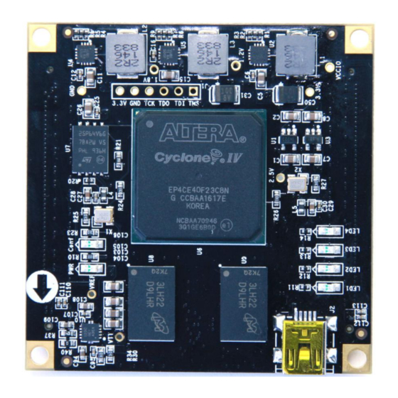
DDR2 connected to the BANK3 and BANK4 of the FPGA.
DDR2 Pin Assignment
Pin Name
DDR2_A[0]
6 / 20
ALINX ALTERA Core Board AC4040 User Manual
Figure 2-2: DDR2 Power for VTT/VREF
FPGA Pin
U10
Amazon Store: https://www.amazon.com/alinx
Pin Name
DDR2_A[11]
FPGA Pin
AB3