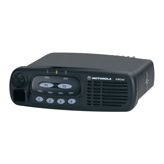
Motorola GM660 Informazioni sul servizio - Pagina 18
Sfoglia online o scarica il pdf Informazioni sul servizio per Radio Motorola GM660. Motorola GM660 34. Gm series professional radio uhf (403-470mhz)
Anche per Motorola GM660: Informazioni sul servizio (32 pagine), Informazioni sul servizio (32 pagine)

2-8
The VCOBIC together with the Fractional-N synthesizer (U3201) generates the required frequencies
in both the transmit and receive modes. The TRB line (U3301 pin 19) determines which tank circuits
and internal buffers are to be enabled. A high level on TRB enables the TX tank and TX output (pin
10), and a low enables the RX tank and RX output (pin 8). A sample of the signal from the enabled
RF output is routed from U3301 pin 12 (PRESC_OUT), via a low pass filter, to pin 32 of U3201
(PREIN).
A steering line voltage (VCTRL) between 2.5V and 11V at varactor diode D3361 will tune the full TX
frequency range (TXINJ) from 136 MHz to 174 MHz, and at varactor diode D3341 will tune the full
RX frequency range (RXINJ) from 181 MHz to 219 MHz. The RX tank circuit uses a Hartley
configuration for wider bandwidth. For the RX tank circuit, an external transistor Q3304 is used for
better side-band noise.
The external RX buffers (Q3301 and Q3302) are enabled by a high at U3301 pin 7 (RX_SWITCH)
via transistor switch Q3303. In the TX mode, the modulation signal (VCOMOD) from the LVFRAC-N
synthesizer IC (U3201 pin 41) is applied to varactor diode D3362, which modulates the TX VCO
frequency via capacitor C3362. Varactor D3362 is biased for linearity from VSF.
4.4
Synthesizer Operation
The complete synthesizer subsystem consists of the low voltage FRAC-N (LVFRACN), the
reference oscillator (a crystal oscillator with temperature compensation), charge pump circuitry, loop
filter circuitry and a DC supply. The output signal PRESC from the VCOBIC (U3301 pin 12) is fed to
U3201 pin 32 (PREIN) via a low pass filter (C3318, L3318 and C3226) which attenuates harmonics
and provides the correct level to close the synthesizer loop.
The pre-scaler in the synthesizer (U3201) is a dual modulus type with selectable divider ratios. The
divider ratio of the pre-scaler is controlled by the loop divider, which in turn receives its inputs via the
SRL. The output of the pre-scaler is applied to the loop divider. The output of the loop divider is
connected to the phase detector, which compares the loop divider´s output signal with the reference
signal. The reference signal is generated by dividing down the signal of the reference oscillator
(Y3261 or Y3263).
The output signal of the phase detector is a pulsed DC signal which is routed to the charge pump.
The charge pump outputs a current at U3201 pin 43 (IOUT). The loop filter (which consists of
R3221-R3223 and C3221-C3224) transforms this current into a voltage that is applied to the
varactor diodes (D3361 for transmit, D3341 for receive) to alter the output frequency of the
appropriate VCO. The current can be set to a value fixed within the LVFRAC-N IC, or to a value
determined by the currents flowing into BIAS 1 (U3201-40) or BIAS 2 (U3201-39). The currents are
set by the value of R3251 and R3252 respectively. The selection of the three different bias sources is
done by software programming.
To reduce synthesizer lock time when new frequency data has been loaded into the synthesizer, the
magnitude of the loop current is increased by enabling the IADAPT pin (U3201-45) for a certain
software programmable time (adapt mode). The adapt mode timer is started by a low to high
transient of the CSX line. When the synthesizer is within the lock range, the current is determined
only by the resistors connected to BIAS 1 and BIAS 2, or by the internal current source. A settled
synthesizer loop is indicated by a high level signal at U3201-4 (LOCK).
The LOCK signal is routed to one of the µP´s ADC inputs (U0101-56). From the measured voltage,
the µP determines whether LOCK is active.
In order to modulate the PLL, the two spot modulation method is utilized. Via U3201 pin 10 (MODIN),
the audio signal is applied to both the A/D converter (low frequency path) as well as the balance
attenuator (high frequency path). The A/D converter changes the low frequency analog modulating
THEORY OF OPERATION
