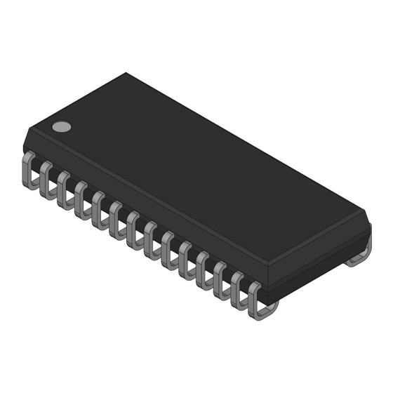
Cypress Semiconductor CY7C199 Scheda tecnica - Pagina 6
Sfoglia online o scarica il pdf Scheda tecnica per Hardware del computer Cypress Semiconductor CY7C199. Cypress Semiconductor CY7C199 17. 32k x 8 static ram

Switching Characteristics
Parameter
READ CYCLE
t
Read Cycle Time
RC
t
Address to Data Valid
AA
t
Data Hold from Address
OHA
Change
t
CE LOW to Data Valid
ACE
t
OE LOW to Data Valid
DOE
t
OE LOW to Low Z
LZOE
t
OE HIGH to High Z
HZOE
t
CE LOW to Low Z
LZCE
t
CE HIGH to High Z
HZCE
t
CE LOW to Power-Up
PU
t
CE HIGH to Power-Down
PD
[10,11]
WRITE CYCLE
t
Write Cycle Time
WC
t
CE LOW to Write End
SCE
t
Address Set-Up to Write End
AW
t
Address Hold from Write End
HA
t
Address Set-Up to Write Start
SA
t
WE Pulse Width
PWE
t
Data Set-Up to Write End
SD
t
Data Hold from Write End
HD
t
WE LOW to High Z
HZWE
t
WE HIGH to Low Z
LZWE
Switching Waveforms
[12, 13]
Read Cycle No. 1
ADDRESS
DATA OUT
PREVIOUS DATA VALID
Notes:
12. Device is continuously selected. OE, CE = V
13. WE is HIGH for read cycle.
Document #: 38-05160 Rev. **
Over the Operating Range
7C199-20
Description
Min.
20
[8]
[8, 9]
[8]
[8, 9]
20
15
15
15
10
[9]
[8]
t
AA
t
OHA
.
IL
[3,7]
(continued)
7C199-25
Max.
Min.
Max.
25
20
25
3
3
20
25
9
10
0
0
9
11
3
3
9
11
0
0
20
20
25
18
20
0
0
0
0
18
10
0
0
10
11
3
3
t
RC
CY7C199
7C199-35
7C199-45
Min.
Max.
Min.
Max.
35
45
35
3
3
35
16
0
0
15
3
3
15
0
0
20
35
45
22
22
30
40
0
0
0
0
22
22
15
15
0
0
15
3
3
DATA VALID
Unit
ns
45
ns
ns
45
ns
16
ns
ns
15
ns
ns
15
ns
ns
25
ns
ns
ns
ns
ns
ns
ns
ns
ns
15
ns
ns
C199–8
Page 6 of 16
