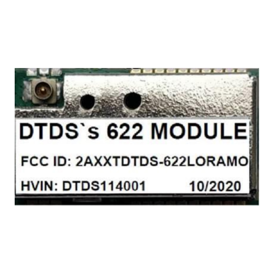
DTDS-622
Pin I/O Description and Serial Configuration
Pin Number
1
2
3
4
5
6
7
8
9
10
11
12
13
14
15
16
17
18
19
20
21
22
23
24
25
26
DTDS2130001 Rev 1.2
User Manual
Pin Name
GND
GND
GND
GPIO/AN0
Reserved
Reserved
Reserved
Reserved
NC
VDD_MAIN
Reserved
Reserved
NC
GND
NC
UART_TxD
UART_RxD
NC
GPIO/AN3
GPIO/AN2
GPIO/AN1
VDD_RF
GND
GND
ANT
GND
Table 1 - Pin Description for DTDS-622 Module
Configuration Items
Baud rate
Data bit
Parity bit
Stop bit
Flow control
Local echo back
Line terminator
Table 2 – Serial/ UART Configuration
Pin Type
-
Ground
-
Ground
-
Ground
I/O
Analog Input/GPIO
-
Reserved for future use
-
Reserved for future use
-
Reserved for future use
-
Reserved for future use
-
No Connection
I
Supply for the Main Board
-
Reserved for future use
-
Reserved for future use
-
No Connection
-
Ground
-
No Connection
O
AT Commands Transmit to Host
I
AT Commands Receive from Host
-
No Connection
I/O
Analog Input/GPIO
I/O
Analog Input/GPIO
I/O
Analog Input/GPIO
I
Supply for the RF Module
-
Ground
-
Ground
I/O
Antenna Signal
-
Ground
Value
115200 bps
8 bits
None
1 bit
None
No
Transmission: CR+LF
Reception: CR+LF
Product Manual
Pin Description
Page 5
October 2020
