- ページ 9
コンピュータ・ハードウェア Alinx ALTER AC4040のPDF ユーザーマニュアルをオンラインで閲覧またはダウンロードできます。Alinx ALTER AC4040 20 ページ。 Core board

SPI Flash pin assignments:
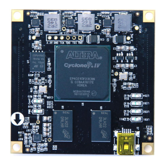
Part 4: FPGA Power Supply
In order for FGPA to work properly, we need to provide 3.3V, 1.8V, 2.5V,
1.2V and VCCIO five-way power for the FPGA. Let's talk about the power pin
portion of the FPGA, which includes the power pins for each bank, the core
voltage pins, the analog voltage, and the phase-locked loop power supply pins.
VCCINT is the FPGA core power supply pin, connected to 1.2V; VCCIO
is the power supply voltage of each BANK of the FPGA, where VCCIO1 is the
power supply pin of the BANK1 of the FPGA. Similarly, VCCIO2~VCCIO8 are
the power supply of the BANK2~BANK8 of the FPGA respectively. In the
AC4040 core board, VCCIO3 and VCCIO4 are connected to 1.8V, because
BANK3 and BANK4 are IOs connected to DDR2. The other BANK (BANK1~2,
BANK5~8) voltages are connected to the adjustable VCCIO, which enables the
BANK IO voltage of the FPGA to be flexibly adjusted. By adjusting the
resistance value of the VCCIO power supply part, different output voltages are
obtained, so that the FPGA core The board's IO level can be applied to different
voltages (the default VCCIO voltage is 3.3V). In addition, with DDR2 on the
core board, a termination power supply VTT and a reference power supply
VREF for DDR2 are required.
The power supply (VCCIO, 1.2V, 1.8V) with three large current
9 / 20
Figure 3-2: M25P64 chip on the FPGA Board
Pin Name
DCLK
nCSO
DATA0
ASDO
Amazon Store: https://www.amazon.com/alinx
ALINX ALTERA Core Board AC4040 User Manual
FPGA Pin
K2
E2
K1
D1
