- ページ 10
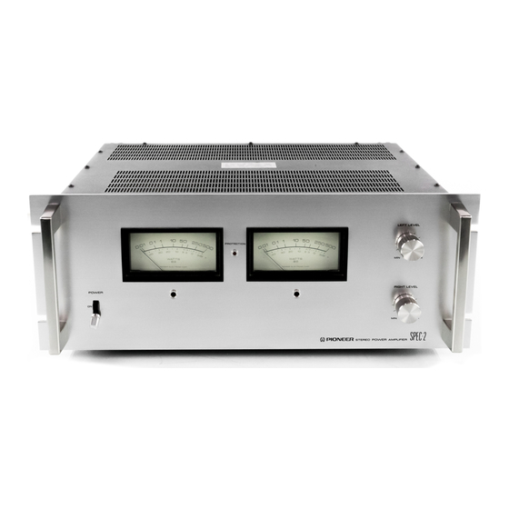
アンプ Pioneer SPEC-2のPDF サービスマニュアルをオンラインで閲覧またはダウンロードできます。Pioneer SPEC-2 50 ページ。 Pioneer spec-2 stereo power amplifier operating instructions
Pioneer SPEC-2 にも: 取扱説明書 (17 ページ)

DC Balance Detector
Q25 and Q26 make up a differential amplifier,
as shown in Fig. 10. The inputs (bases) of these
transistors are connected to the left and right
power amplifier.
If
for
some reason the DC
balance of the power stage is upset, a potential
difference arises in the differential amplifier input
signal, unbalancing q25 and Q26 collector currents.
When one of the collector potentials becomes
lower than Q27 base potential, this base potential
is dissipated through D1 or D2, q27 switches ON,
and relay and lamp drives operate.
r- -----
i
i t c l l
r - - - - - - - - J
I
I
I
L -
--:E---..i
Fig. 10 DC Balance Detector Circuit
4 . 4 S U R G E C U R R E N T S U P P R E S S O R C I R C U I T S
A toroidal core power transformer is used in the
SPEG2, which while possessing compactness and
a large handling capacity, also exhibits extremely
low intemal resistance. In combination with the
four 15,000pF electrolytic capacitors forming the
power supply, surge current accompanying power
switch operation can reach a maximum of 3004.
The power supply can therefore be damaged unless
protective measures are taken.
The main sources of surge current generation are
power transformer excitation current and power
supply electrolytic capacitor charging current.
Two surge suppressor circuits are employed in the
SPEC-2, one each in the primary and secondary
power transformer
circuits.
These circuits are
shown in Fig. 11.
Power transformer excitation current is handled
by the relay surge suppressor circuit
at the
primary side. When the power switch is turned
ON, the current passes through R2 & D1 and
charges C1, therefore it does not flow through the
relay drive coil immediately, and RLl
remains
OFF. The transformer excitation current flows
through
R1 during
this interval. After. C1 is
completely
charged, current flows in the RL1
+83 drive coil switching it ON, and R1 is shorted.
The surge suppressor circuit in the
secondary side of the power trans-
former is designed to handle the
electrolytic capacitor charging cur-
rent. When the power switch is
turned ON, RL2 and RLB remain
OFF due to protection circuit op-
eration. Consequently, the current
passes through R3 and R4, gradu-
ally charging the electrolytic capaci-
tors through a bridge type rectifier
circuit. RL2 or RLB is switched ON
when charging has been completed,
gving the normal operating mode.
By employing these circuits, surge
current is limited to approximately
40 A.
tlectrolytic
c a p a c i t o r
Poror
amplilicr
+ B l
+
t lectrolytic
catac ito t
Relay and lanp
d riv ors
1 0
Fig. 11 Surge Current Suppressor Circuit
-Bl
