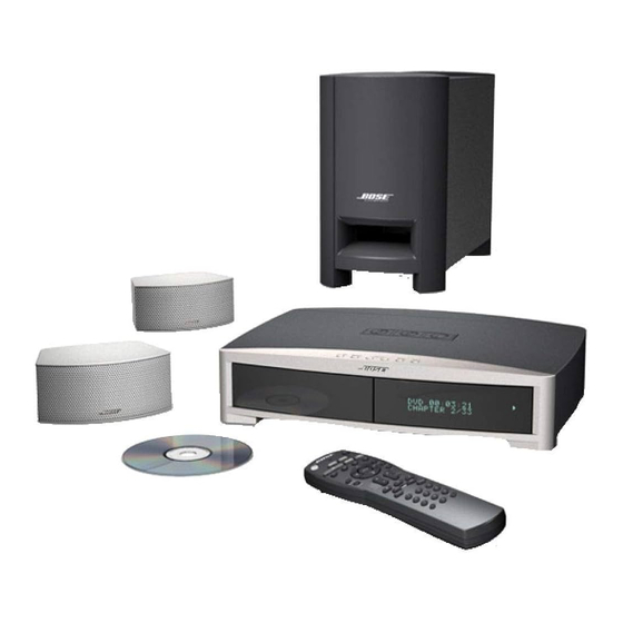
Bose 3-2-1 문제 해결 매뉴얼 - 페이지 23
{카테고리_이름} Bose 3-2-1에 대한 문제 해결 매뉴얼을 온라인으로 검색하거나 PDF를 다운로드하세요. Bose 3-2-1 28 페이지. Home entertainment system
Bose 3-2-1에 대해서도 마찬가지입니다: 소유자 매뉴얼 (44 페이지), 빠른 설정 매뉴얼 (1 페이지)

When the /STDBYout signal is high, the MODE pin will be either within the 3.3-6.4 volt range
(mute), or near VRAW (active), as controlled by the MUTE signal and Q450, D450. When
MUTE is high, Q450 saturates, causing the MODE voltage to be driven to approximately 5.4
volts. R450 assures the MUTE signal is active any time the DSP (U7000) is not driving it.
The open-collector diagnostic outputs of the three amplifier IC's are summed into the /DIAG
signal to the DSP (U7000 [sheet 1, B/C 4/5]). R453 [sheet 5, C7] pulls the signal to logic false
(high) when none of the amplifiers is asserting the signal. Currently /DIAG is unused by the
DSP.
The Clip signals of the amplifier IC's driving the array speakers (U150, U250) are summed into
the /ARRAYCLIP signal. R454 [sheet 5, D2] holds the signal false (high) if neither amplifier IC
is asserting the clip signal. A similar arrangement is used for the bass amplifier with the /
BASSCLIP signal.
2.2.2.5 Digital-to Analog Signal conversion and conditioning
Processed audio signals are converted to amplifier drive signals by the DAC portion of the
Codec (CS4228), U4000 [sheet 2, C/D2]. The single-ended outputs of U4000 have a full-scale
output of nominally 1.31 Vrms. They also have significant out-of-band noise as well as the
expected sigma-delta conversion noise due the IC's location in the digital portion of the circuit.
Resistor arrays R4300, R4301, R4302 [B2] serve to terminate the negative signal of the power
amplifier differential inputs and provides the source impedance for the first stage of the second-
order low-pass filter. The Capacitors C4300-11 provide both the switching noise suppression on
the individual signal and one of the two poles for the second-order lowpass filter.
Resistor arrays R150 [sheet 5, C4], R250 [B4], R350 [B8] increase the source impedance of the
second portion of the filter. The shunt resistance of R151 and similar and the shunt capacitance
of C158 and similar form the second pole.
Analog output gain for a 0dbFS digital signal...
•
DAC output
•
Filter Gain
•
Amplifier Gain
•
Total Gain
•
Max amplitude
Note that DSP gain managers limit the signals to avoid clipping, which is likely to occur beyond
11 volts peak.
2.2.2.6 Analog-to Digital Conversion
The analog inputs (J7100, pins 2, 3, 5, 6 [sheet 3, C7]) are coupled to the ADC differential input
of U4000 [sheet 2, C/D2] through a RC t-network which utilizes the inherent element matched
values of quad resistor packs R1001 and R1005. This provides good common-mode rejection
on the inputs as well as providing a lowpass filter function.
The A/D conversion sample rate is determined by the SHARC_CLK providing a 128Fs master
clock to the converter (33.333MHz/6 = 5.56MHz) rate which ultimately yields a sample rate of
43.4kHz.
THEORY OF OPERATION
1.3Vrms
-8dB
26dB
18dB (8x)
10.4 volts RMS or 14.7 volts peak
23
