EPC EPC9144 빠른 시작 매뉴얼 - 페이지 2
{카테고리_이름} EPC EPC9144에 대한 빠른 시작 매뉴얼을 온라인으로 검색하거나 PDF를 다운로드하세요. EPC EPC9144 9 페이지. Development board for a 15 v high current pulsed laser diode driver
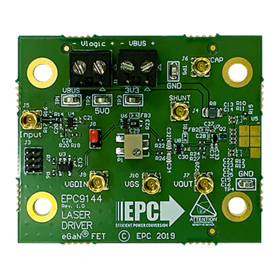
QUICK START GUIDE
DESCRIPTION
The EPC9144 development board is primarily intended to drive laser
diodes with high current pulses with total pulse widths as short as 1.2 ns
and currents of up to 28 A. The board is designed around the EPC2216
enhancement mode (eGaN®) field effect transistor (FET). The EPC2216
is an AEC-Q101 automotive qualified 15 V FET capable of current pulses
up to 28 A. The EPC9144 ships with the EPC9989 interposer board. The
EPC9989 is a collection of break-away 5 mm x 5 mm square interposer
PCBs with footprints for different lasers, RF connectors, and a collection
of other footprints designed for experimentation with different loads.
The use of the interposers allows many different lasers or other loads to be
mounted while still being able to use the EPC9144. Laser diodes or other
loads are not included, and must be supplied by the user.
The EPC9144 comprises a ground-referenced EPC2216 eGaN FET driven
by a Texas Instruments LMG1020 gate driver. The printed circuit board
is designed to minimize the power loop inductance while maintaining
mounting flexibility for the laser diode or other load. It includes multiple
on-board passive probes for voltages, and is equipped with MMCX con-
nections for input and sensing. In addition, the board includes a narrow
pulse generator capable of sub-nanosecond operation, or the user can
simply feed the gate drive directly via removal of a resistor. As shipped,
the board is designed to operate from 3.3 V logic, but is equipped with
both a logic level translator and a differential receiver to accommodate
different use cases. Finally, the board can also be used for other applica-
tions requiring a ground-referenced eGaN FET, e.g. Class E amplifiers or
similar. A complete block diagram of the circuit is given in figure 1, and a
detailed schematic in figure 4.
For more information on the EPC2216 eGaN FETs, please refer to the data-
sheet available from EPC at www.epc-co.com. The datasheet should be
read in conjunction with this quick start guide.
SETUP AND OPERATION
Development board EPC9144 is easy to set up to evaluate the perfor-
mance of the EPC2216 eGaN FET. Refer to Figure 2 for proper connect and
measurement setup and follow the procedure below:
1. Review laser safety considerations. Observe all necessary laser safety
requirements including the use of personal protection equipment
(PPE) as required. Refer to qualified safety personnel as necessary.
2. With power off, install laser diode U2 or other load. The use of one of
the interposers from the included EPC9989 may be used to mount the
laser or other load, and this is discussed in the section LASER DIODE
AND LOAD CONSIDERATIONS for further information.
3. With power off, connect the input power supply bus to +V
ground / return to –V
BUS
4. With power off, connect the logic supply (7-12 V V
and ground return to –V
5. With power off, connect the signal pulse generator to the input J5. J5
is terminated with 50 Ω on the EPC9144, and is designed for a 3.3 V
logic input as shipped. This can be changed as discussed in this guide.
6. Connect the remaining measurement MMCX outputs to an oscil-
loscope, using 50 Ω cables and with the scope inputs set to 50 Ω
impedance. See section MEASUREMENT CONSIDERATIONS for more
information, including the attenuation values for each output.
EPC – THE LEADER IN GaN TECHNOLOGY |
(J1) or GND.
) to +V
DC
(J2) or GND.
Logic
WWW.EPC-CO.COM
Table 1: Performance Summary (T
Symbol
Gate drive and
V
Logic
Bus input voltage
V
BUS
Z
Input impedance
IN
V
Input pulse range
INPUT
T
Input pulse width
Pin
SAFETY WARNING: This board is capable of driving laser diodes to generate high
peak power optical pulses. Such pulses are capable of creating permanent vision
damage. User must follow proper laser safety procedures to prevent vision damage.
+
V
BUS
–
Input (J5)
V7
in
7. Turn on the logic supply voltage to a value within the specification.
8. Turn on the bus voltage to a value within the specification.
9. Turn on the pulse source and observe switching operation via the
(J1) and
BUS
outputs and any additional desired probing. Laser diode output
may be observed with an appropriate electro-optical receiver.
(J2)
Logic
10. Once operational, adjust the bus voltage, input pulse width, and
pulse repetition frequency (PRF) as desired within the operating
range and observe the system behavior.
11. For shutdown, please follow steps in reverse.
NOTE: When measuring the high frequency content switch node, care must be
taken to avoid long ground leads. Measure the switch node by placing the
oscilloscope probe tip through the large via on the switch node (designed for this
purpose) and grounding the probe directly across the GND terminal provided.
See
EPC measurement applications note.
| COPYRIGHT 2019 |
Demonstration System EPC9144
= 25°C) EPC9144
A
Parameter
Conditions
logic supply
range
J5 input
CAP (J6)
Narrow pulse
generator
(optional)
V
GS
(J9)
+
LDO
–
Figure 1: Block diagram of EPC9144 development board
Min
Nom Max Units
6
12
V
0
12*
V
50
Ω
0
5
V
1
ns
D
clmp
U
2
V
(J7)
OUT
Q1
V
GS
(J10)
| 2