CIRCUIT DESIGN CDP-TX-07MP 운영 매뉴얼 - 페이지 5
{카테고리_이름} CIRCUIT DESIGN CDP-TX-07MP에 대한 운영 매뉴얼을 온라인으로 검색하거나 PDF를 다운로드하세요. CIRCUIT DESIGN CDP-TX-07MP 14 페이지. Uhf narrow band radio data module
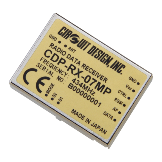
PIN DESCRIPTION
Common to CDP-RX-07M and CDP-RX-07MP
Pin-
Pin-No.
I/O
Name
CN1-1
DATA
O
CN1-2
AF
O
CN1-3
RSSI
O
CN1-4
CTRL
CN1-5
VCC
CN1-6
GND
CN2-1
ANT
CN2-2
GND
JP1
JP2
OG_CDP-RX-07M_v20e
The data signal output
The terminal is pulled up with a resistor.
The output signal level is 0 to Vcc.
The AF signal output terminal
The signal output level is -10.5dBm typ.
(Fm=1 kHz /Fmod=+/-3 kHz, 100 k ohm)
The receiving level output
The level indicates the strength of RF level.
Note that the output voltage may be reduced
depending on the load impedance to be
connected.
The power on/off control terminal (Low active).
A voltage of VCC-1.8 V or lower voltage makes
the circuit active and VCC-0.6 V or higher
disables the circuit.
Please control this terminal with an open-
I
collector or open-drain output.
Note that leakage current will flow if there is a
potential difference between VCC and the
CTRL.
Do not apply a voltage of VCC+0.3 V or higher
to the CTRL pin.
The power supply terminal.
-
Operates on 3.0 to 14 V.
The ground.
-
Connect to the ground of the control board.
The antenna terminal Connect an antenna with
50 ohm impedance.
-
The ground terminal for the antenna.
Solder jumpers for frequency channel setting.
This terminal is pulled-up to the internal power
supply.
I
Ch3 (JP1-Open JP2-Open)
Ch2 (JP1-Short JP2-Open)
Ch1 (JP1-Open JP2-Short)
Ch0 (JP1-Short JP2-Short)
Description
5
OPERATION GUIDE
Equivalent internal circuit
Circuit Design, Inc.
.