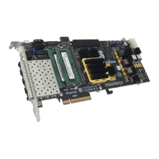
Digilent NetFPGA-SUME 참조 매뉴얼 - 페이지 8
{카테고리_이름} Digilent NetFPGA-SUME에 대한 참조 매뉴얼을 온라인으로 검색하거나 PDF를 다운로드하세요. Digilent NetFPGA-SUME 20 페이지.

NetFPGA-SUME™ Reference Manual
When the input voltage falls below 9 volts, or the power switch transitions to the "OFF" position, the LTC2974s
perform a time-based off sequence and the rails come down in the following order:
1. MGTVAUX
2. VCC1V5, QDRVTT, and DDRVTT
3. VCC3V3
4. MGTAVTT
5. MGTAVCC
6. VCC2V0
7. VCC1V8
8. VCC1V0
The LTC2974s constantly monitor the output voltage, current, and temperature associated with each channel
(supply rail). This information, referred to as telemetry data, is used to determine the on status of each supply rail,
as well as monitor for fault and warning conditions. When a fault or a warning occurs, the FPGA application may be
notified via an interrupt that is signaled by the LTC2974's ALERTB, AUXFAULTB, or FAULTB1 pins. The FPGA
application may then read (using I2C) one or more of the LTC2974 status registers (defined in the datasheet) to
determine the source of the fault or the warning. The output voltage, current, power, and temperature associated
with any channel may also be read using the applicable PMBUS (I2C) commands, which are defined in the LTC2974
datasheet.
In order to generate faults and warnings, each channel of the LTC2974 must be configured with a nominal output
voltage, under voltage warning limit, over voltage fault limit, under current warning limit, over current warning
limit, over current fault limit, under current fault limit, under temperature warning limit, under temperature fault
limit, and over temperature fault limit. Tables 2 and 3 describe the voltage and current limits as pre-configured by
Digilent during the manufacturing process.
Supply
Under Voltage
Rail
Fault Limit
VCC1V0
0.9V
VCC1V8
1.62V
VCC2V0
1.8V
MGTAVCC
0.9V
MGTAVTT
1.08V
VCC3V3
2.97V
VCC1V5
1.35V
MGTVAUX
1.62V
DDRVTT
N/A
QDRVTT
N/A
Copyright Digilent, Inc. All rights reserved.
Other product and company names mentioned may be trademarks of their respective owners.
Figure 8. Power ON/OFF sequence.
Under Voltage
Nominal
Warning Limit
Voltage
0.925V
1.0V
1.665V
1.8V
1.85V
2.0V
0.925V
1.0V
1.11V
1.2V
3.0525V
3.3V
1.3875V
1.5V
1.665V
1.8V
N/A
0.75V
N/A
0.75V
Table 2. Voltage fault and warning limits.
Overvoltage
Overvoltage Fault
Warning Limit
Limit
1.075V
1.1V
1.935V
1.98V
2.15V
2.2V
1.075V
1.1V
1.29V
1.32V
3.5475V
3.63V
1.6125V
1.65V
1.935V
1.98V
N/A
N/A
N/A
N/A
Page 8 of 18
