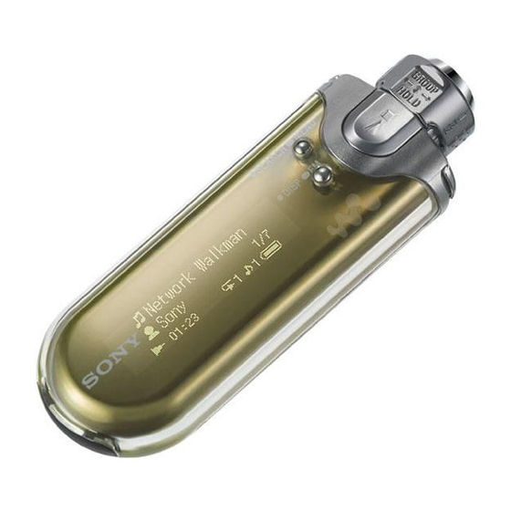
Sony NW-E505 - Network Walkman 서비스 매뉴얼 - 페이지 12
{카테고리_이름} Sony NW-E505 - Network Walkman에 대한 서비스 매뉴얼을 온라인으로 검색하거나 PDF를 다운로드하세요. Sony NW-E505 - Network Walkman 32 페이지. Portable ic audio player
Sony NW-E505 - Network Walkman에 대해서도 마찬가지입니다: 운영 지침 (2 페이지), 사양 (2 페이지), 제한 보증 (1 페이지), 사용 시 참고 사항 (1 페이지), 서비스 매뉴얼 (30 페이지), 빠른 시작 매뉴얼 (3 페이지)

NW-E503/E505/E507
Ver. 1.5
Note on Schematic Diagram:
• All capacitors are in µF unless otherwise noted. (p: pF) 50 WV
or less are not indicated except for electrolytics and tantalums.
• All resistors are in Ω and
1
/
W or less unless otherwise speci-
4
fied.
•
%
: indicates tolerance.
• C : panel designation.
•
: B+ Line.
• Voltages and waveforms are dc with respect to ground under
no-signal (detuned) conditions.
no mark : PLAY
: Impossible to measure
*
• Voltages are taken with a VOM (Input impedance 10 MΩ).
Voltage variations may be noted due to normal production toler-
ances.
• Waveforms are taken with a oscilloscope.
Voltage variations may be noted due to normal production toler-
ances.
• Circled numbers refer to waveforms.
• Signal path.
E
: PLAY BACK
a
: DIGITAL OUT
k
: DIGITAL IN
d
: TUNER
F
: AUDIO
• Waveforms
1
IC400 <zcm (XTAL)
44.3 ns
500 mV/DIV, 20 ns/DIV
2
IC400 <zvz (TX)
62.5 ns
1 V/DIV, 20 ns/DIV
3
IC401 8 (OSCOUT)
16.3 µ s
500 mV/DIV, 20 µ s/DIV
12
SECTION 4
DIAGRAMS
2.2 Vp-p
3.4 Vp-p
1.5 Vp-p
Note on Printed Wiring Board
• X : parts extracted from the component side.
• Y : parts extracted from the conductor side.
•
: Pattern from the side which enables seeing.
Caution:
Pattern face side: Parts on the pattern face side seen from
(Side A)
the pattern face are indicated.
Parts face side:
Parts on the parts face side seen from
(Side B)
the parts face are indicated.
• MAIN board is multi-layer printed board.
However, the patterns of intermediate-layer have not been in-
cluded in the diagram.
*
Replacement of IC400 on MAIN board requires a special
tool.
• Lead Layouts
Lead layout of conventional IC
surface
CSP (Chip Size Package)
