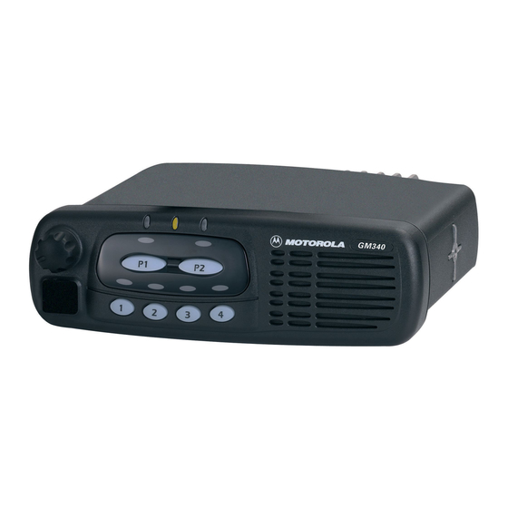
Motorola GM640 서비스 정보 - 페이지 20
{카테고리_이름} Motorola GM640에 대한 서비스 정보을 온라인으로 검색하거나 PDF를 다운로드하세요. Motorola GM640 32 페이지. Gm series professional radio uhf (403-470mhz)
Motorola GM640에 대해서도 마찬가지입니다: 서비스 정보 (34 페이지), 사용자 설명서 (28 페이지), 서비스 정보 (32 페이지)

2-10
5.3
Driver Stage
The following stage is an enhancement-mode N-Channel MOSFET device (Q4431) providing a gain
of 10dB. This device also requires a positive gate bias and a quiescent current flow for proper
operation. The voltage of the line Bias_2_UHF_PA_1 is set in transmit mode by the ASFIC and fed to
the gate of Q4431 via the resistive network R4632, R4631, R4485 and R4486. This bias voltage is
also tuned in the factory. If the transistor is replaced, the bias voltage must be tuned using the
Customer Programming Software (CPS). Care must be taken not to damage the device by exceeding
the maximum allowed bias voltage. The device's drain current is drawn directly from the radio's DC
supply voltage input, A+, via L4421.
5.4
Final Stage
The final stage uses the bipolar device Q4441. The device's collector current is also drawn from the
radio's DC supply voltage input. To maintain class C operation, the base is DC-grounded by a series
inductor (L4441) and a bead (L4440). A matching network consisting of C4441-C4444, C4491 and
two striplines transforms the impedance to 50 Ohms and feeds the directional coupler.
5.5
Directional Coupler
The Bi-directional coupler is a microstrip printed circuit, which couples a small amount of the forward
and reverse power of the RF power from Q4441. The coupled signal is rectified to an output power
proportional DC voltage by the diodes D4451 & D4452 and sent to the RFIN of PCIC. The PCIC
controls the gain of stage U4401 as necessary to hold this voltage constant, thus ensuring the
forward power out of the radio to be held to a constant value.
5.6
Antenna Switch
The antenna switch consists of two PIN diodes, D4471 and D4472. In the receive mode, both
diodes are off. Signals applied at the antenna jack J4401 are routed, via the harmonic filter, through
network L4472, C4474 and C4475, to the receiver input. In the transmit mode, K9V1 turns on
Q4471 which enables current sink Q4472, set to 96 mA by R4511 and VR4471. This completes a
DC path from PASUPVLTG, through L4437, D4471, L4472, D4472, L4473, R4496 and the current
sink, to ground. Both diodes are forward biased into conduction. The transmitter RF from the
directional coupler is routed via D4471 to the harmonic filter and antenna jack. D4472 also
conducts, shunting RF power and preventing it from reaching the receiver port (RXIN). L4472 is
selected to appear as a broadband Lambda/4 wave transmission line, making the short circuit
presented by D4472 appear as an open circuit at the junction of D4472 and the receiver path.
5.7
Harmonic Filter
Inductors L4491, L4492, L4493 and capacitors C4448, C4492,C4494, C4496 and C4498 form a
low-pass filter to attenuate harmonic energy of the transmitter to specifications level. R4491 is used
to drain electrostatic charge that might otherwise build up on the antenna. The harmonic filter also
prevents high level RF signals above the receiver passband from reaching the receiver circuits,
improving spurious response rejection.
THEORY OF OPERATION
