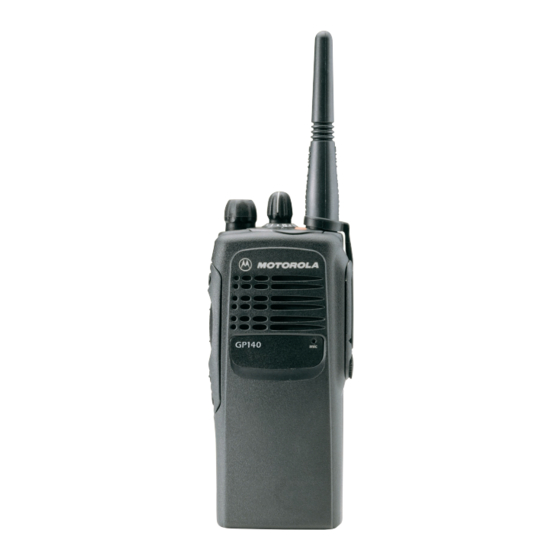
Motorola GP280 서비스 정보 - 페이지 13
{카테고리_이름} Motorola GP280에 대한 서비스 정보을 온라인으로 검색하거나 PDF를 다운로드하세요. Motorola GP280 30 페이지. Professional radio, power distribution and controller
Motorola GP280에 대해서도 마찬가지입니다: 사용자 설명서 (46 페이지), 서비스 정보 (32 페이지), 사용자 설명서 (46 페이지), 서비스 정보 (30 페이지)

VHF Receiver
3.0
VHF Receiver
The VHF receiver consists of a front end, back end, and automatic gain control circuits. A block
diagram of the VHF receiver is shown in Figure 2-2. Detailed descriptions of these features are
contained in the paragraphs that follow.
Antenna
Pin Diode
Antenna
Switch
RF Jack
3.1
Receiver Front-End
(Refer to Figure 2-2 and the VHF Receiver Front End schematic diagram)
The RF signal is received by the antenna and applied to a low-pass filter consisting of L3531, L3532,
C3532 to C3563. The filtered RF signal is passed through the antenna switch. The antenna switch
circuit consists of two pin diodes (D3521 and D3551) and a pi network (C3531, L3551, and
C3550).The RF signal is then applied to a varactor tuned bandpass filter which consists of L3301,
L3303, C3301 to C3304, and D3301. The filter is tuned by applying a control voltage to the varactor
diode (D3301) in the filter.
The bandpass filter is electronically tuned by the DACRx from IC 404 which is controlled by the
microprocessor. Depending on the carrier frequency, the DACRx supplies the tuned voltage to the
varactor diodes in the filter. Wideband operation of the filter is achieved by shifting the bandpass
filter across the band.
The output of the bandpass filter is coupled to the RF amplifier transistor Q3302 via C3306. After
being amplified by the RF amplifier, the RF signal is further filtered by a second varactor tuned
bandpass filter, consisting of L3305, L3306, C3311 to C3314 and D3302.
Varactor
RF Amp
Tuned Filter
First LO
from FGU
Control Voltage
from ASFIC
Recovered Audio
Squelch
RSSI
16.8 MHz
Reference Clock
Figure 2-2 VHF Receiver Block Diagram.
Varactor
Tuned Filter
AGC
Demodulator
IC
IF
SPI Bus
Crystal
Mixer
Filter
Synthesizer
Second
LO VCO
2-3
