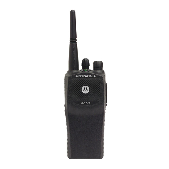
Motorola CP180 서비스 정보 - 페이지 13
{카테고리_이름} Motorola CP180에 대한 서비스 정보을 온라인으로 검색하거나 PDF를 다운로드하세요. Motorola CP180 46 페이지. Uhf2 (438-470mhz)
Motorola CP180에 대해서도 마찬가지입니다: 기본 사용 설명서 (16 페이지), 기본 사용 설명서 (16 페이지), 기본 사용 설명서 (18 페이지), 자세한 서비스 매뉴얼 (28 페이지), Cps/튜너 설치 매뉴얼 (6 페이지), 서비스 정보 (46 페이지)

UHF Transmitter
3.3
Harmonic Filter
The harmonic filter consists of components C130-C136 and L130-L132. The harmonic filter is a
seven-pole Chebychev low-pass configuration, optimized for low insertion loss, with a 3 dB
frequency of approximately 600 MHz and typically less than 0.8 dB insertion loss in the passband.
3.4
Antenna Matching Network
The harmonic filter presents a 50Ω impedance to antenna jack J140. A matching network, made up
of C140-C141 and L140, is used to match the antenna impedance to the harmonic filter. This
optimizes the performance of the transmitter and receiver into the impedance presented by the
antenna, significantly improving the antenna's efficiency.
3.5
Power Control
The power control circuit is a dc-coupled amplifier whose output is the dc gate bias voltage (VGG)
applied to the two stages of the RF power amplifier U110.
The output power of the transmitter is adjusted by varying the setting of the power-set DAC
contained in the ASFICcmp IC (DACG, U451 pin 6). This PWR_SET voltage is applied to
U150 pin 3.
Stage U150-2 compares the voltage drop across current sense resistor R150 to the voltage drop
across resistor R151 caused by current flow through Q150, and adjusts its output (pin 7) to maintain
equal voltages at pins 5 and 6. Thus the current flow through Q150, and hence its emitter voltage, is
proportional to the current drawn by stage U110, which is in turn proportional to the transmitter
output power. The emitter voltage of Q150 is applied to U150 pin 2, where it is compared to the
power set voltage PWR_SET at pin 3.
The output of U150 pin 1 is divided by R110 and R111 and applied as a gate voltage to the power
amplifier U110. By varying this gate voltage as needed to keep the voltages at U150 pins 2 and 3
equal, power is maintained at the desired setting. Excessive final current, for example due to
antenna mismatch, causes a lowering of the voltage at U150 pin 6, an increased voltage at pin 2,
and a lowering of the voltage at pin 1 and of the gate voltage VGG. This prevents damage to the final
stage due to excessive current.
2-5
