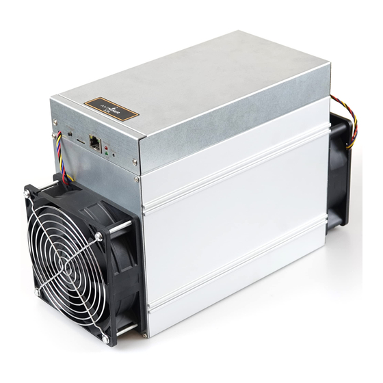
ASIC Bitmain Antminer S9K 유지 관리 매뉴얼 - 페이지 3
{카테고리_이름} ASIC Bitmain Antminer S9K에 대한 유지 관리 매뉴얼을 온라인으로 검색하거나 PDF를 다운로드하세요. ASIC Bitmain Antminer S9K 13 페이지.
钳位电路输出端
EC39 为 3.5V
钳位电路输出端 EC39 为 3.5V
Clamping circuit output EC39 is 3.5V
The flow direction of CLKO signal is generated by Y1 25M crystal oscillator, which is transmitted from chip U1 to chip U30; it is generated by Y2 25M
crystal oscillator, and is transmitted from chip U31 to chip U60. When standby and computing, the voltage is 0.9V.
Signal CO (CI, C0) enters from the Pin 7 at port IO (J4), and is then transmitted from chip U1 to chip U60; when the IO line is not inserted, the voltage is 0,
and the voltage is 1.8V when computing.
Signal RI (R1, RO) returns from chip U60 to chip U1, and then returns to the control board from the pin (J4) 8 at IO port; when the IO signal is not inserted,
the voltage is 1.8V, and the voltage is 1.8V when computing.
Signal BO (BI, BO) flows from chip U1 to U60 to lower the level; the voltage is 0V when there is no IO line inserted and during standby, there is a pulse
signal around 0.3 when computing, generally if no voltage can be measured, it is normal.
Signal NRSTO (NRSTO, NRSTI) enters from pin (J4)) 3 at IO port, and is then transmitted from chip U1 to chip U60; the voltage is 0V when there is no IO
signal inserted and during standby, and the voltage is 1.8V when computing.
2.2 Key circuits of the S9K S9SE computing board
2.2.1 Schematic diagram of U122 power management
3
S9k S9SE Maintenance Guide