Alinx ALTER AC4075 User Manual - Page 6
Browse online or download pdf User Manual for Computer Hardware Alinx ALTER AC4075. Alinx ALTER AC4075 19 pages. Core board
address lines and control lines, and VTT voltage VREF are 0.9V. Figure 2-2
detailed the power supply schematic below:
Figure 2-3: DDR2 Power Circuit on the Core Board
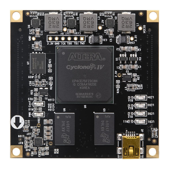
DDR2 connected to the BANK3 and BANK4 of the FPGA.
DDR2 Pin Assignment
Pin Name
DDR2_A[0]
DDR2_A[1]
DDR2_A[2]
DDR2_A[3]
6 / 19
ALINX ALTERA Core Board AC4075 User Manual
Figure 2-2: DDR2 Power for VTT/VREF
FPGA Pin
R14
AB5
T16
U17
Amazon Store: https://www.amazon.com/alinx
Pin Name
DDR2_A[11]
DDR2_A[12]
DDR2_BA[0]
DDR2_BA[1]
FPGA Pin
AA3
AA20
AA6
R16