EPC EPC9144 Quick Start Manual - Page 5
Browse online or download pdf Quick Start Manual for Motherboard EPC EPC9144. EPC EPC9144 9 pages. Development board for a 15 v high current pulsed laser diode driver
QUICK START GUIDE
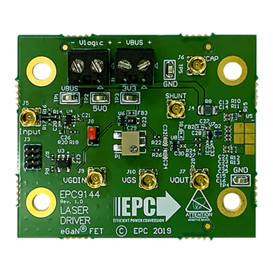
Table 2: Key properties of the MMCX test points for ease of reference
Designator
PCB label
J6
CAP
J4
SHUNT
Not used
J7
V
OUT
J9
V
GDIN
J10
V
GS
MODIFICATIONS
Narrow pulse generator
Many signal generators cannot produce an accurate, short pulse. The
EPC9144 includes circuitry to obtain narrow output pulses, following
a method given in Section 8.2.2.2 of the Texas Instruments LMG1020
data sheet. This method is based on the Jim Williams circuit in [REF].
This is controlled through trimmer potentiometer P1. The pulse range is
approximately ~1.2 ns to ~20 ns. The minimum width is determined from
the point at which the gate drive pulses to Q1 begin to drop out. This
boundary is determined by the LMG1020 gate driver, and may vary with
temperature or other factors. The input pulse with to the narrow pulse
generator should be at least 10 ns longer than the desired pulse width
for reliable operation. The user should consult with Texas Instruments
(Figures 7 & 8) if operating near the IC specification boundaries.
For greater flexibility, e.g. when the user would like to use variable
pulse width, the user may disable the narrow pulse generator by
simply removing R27 (Fig. 6). Once done, the input to the gate drive
IC will follow the input pulse from the user's pulse source. This allows
variable pulse generation and very high frequency operation given the
appropriate user-generated input.
Pulse sources
The EPC9144 comes with out-of-the-box support for 3.3 V logic
levels input to J5. The input includes a logic level translator U4 to
accommodate lower voltage logic, which is often used for high speed
designs. To accommodate lower voltage logic levels, simply change R18
(Fig. 6), which sets the voltage at U4 pin 5, and thereby determines the
input logic level.
For very high speed systems, differential signaling protocols
such as LVDS or CML are commonly used. To accommodate this,
the EPC9144 has a flexible differential receiver U3, whose inputs
is available via J3. In order to make use of the differential input
capability, the jumper on J8 must be moved from the SE position
to the DIFF position. This will disable the J5 input and enable the
J3 differential input (Fig 6.). U3 is configured for a 100 Ω differential
EPC – THE LEADER IN GaN TECHNOLOGY |
Attenuation
Description
factor
Bus capacitor
voltage (VCHARGE on
41 V/V
schematic)
Shunt voltage
Not used
Q1 drain voltage
41 V/V
Q1 drain voltage
41 V/V
Gate drive input
20 V/V
Q1 gate voltage
20 V/V
WWW.EPC-CO.COM
| COPYRIGHT 2019 |
impedance with a 0.85 V DC bias offset, which should accommodate
typical LVDS transmitters. These parameters can be modified as
needed to accommodate various differential signaling schemes.
This application note
is useful to configure U3 for different needs.
Clamping diodes
The EPC9144 shipped configured as a dual edge control driver.
When the FET Q1 is turned off, energy stored in the stray power loop
inductance can cause a Q1 drain voltage spike to exceed the device
ratings. In order to reduce the voltage spike, a diode-connected
EPC2036 FET Q2 is used to help clamp the drain node. There are
also provisions for up to two other clamping diodes D1 and D2.
While diodes Q2, D1 and D2 can provide some protection to FET Q1
and laser U2, they have parasitic inductance and capacitance that
can reduce performance at the very fastest speeds. Hence, only Q2
is populated, and it is left to the user to determine whether they are
beneficial for any particular application. D1, D2, and Q2 locations are
on the bottom side of the EPC9144 PCB.
NOTE. The EPC9144 demonstration board does not have any thermal
protection on board.
Location of
J3 input
R27
(DIFF)
Figure 6: Remove R27 to disable the onboard narrow pulse generator and
drive the gate drive from the pulse source.
Demonstration System EPC9144
J5 input
Location of
(SE)
R27
| 5