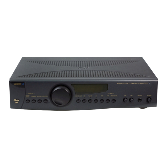
Arcam Alpha 10 Service Manual
Browse online or download pdf Service Manual for Amplifier Arcam Alpha 10. Arcam Alpha 10 19 pages. Arcam digital radio tuner handbook
Also for Arcam Alpha 10: Handbook (15 pages), Handbook (11 pages)

ALPHA 10/10P SERVICE MANUAL
H
AL
ALPHA 10/10P SERVICE MANUAL
CIRCUIT DESCRIPTION
The mother PCB is common for both the A10 and A10P with the exception of the input mode switch and pre-amp
output mute relay which are only fitted to the A10 and the power/standby LED and links to parallel the input
connections to what would otherwise be the pre-amp output for use with a mono link. The amplifier is based on the
D290/Alpha 9 design but with lower gain, a higher current and higher voltage driver stage and a high power output
stage. The current servo has been improved over the Alpha 9 to be output device independent. A micro supervises
rd
the amplifier state, switch state and remote control functions. Provision is made for an additional 3
channel PCB to
be added with power supply and protection circuitry access.
Input stage
The input connections are taken either from the pre-amp connector, LK12X, or the external power amp input on the
A10 depending on the position of SW1. On the A10P, the input is taken from the external power amp input only with
provision for a mono shorting link by having two parallel input connectors. On the A10, there is a mute relay on the
pre-amp outputs which are always connected to the pre-amp connector, LK12X.
The signal is passed through a low pass filter with a -3dB point of 550KHz at normal gain and 740KHz at low gain.
The gain is selected by SW2. C72 and C74 are d.c. blocking capacitors with a -3dB point of 0.7Hz. A d.c. error
correction current is injected into the base of Q19 and 26 from the voltage servo Z3 and 4, to null any voltage offset at
the amplifier output.
The input and voltage amplifier stages both run off regulated 15 Volt suppies. The input stage is an NPN differential
input, Q18, 19, 25 and 26, with an adjustable current source, Q21 and 28 which sets the quiescent current through all
the stages but specifically the output stage. C37, R58, C49 and R66 keep the input stage and voltage amplifier stable.
Q52, 53, 54 and 55 form a current mirror to ensure that the differential input is balanced during normal operation.
Voltage Amplifier
The voltage amplifier consists of another differential pair, Q48, 49, 50 and 51. Q48 and 50 are the positive pulling side
of the voltage amplifier output and Q49 and 51 pull negative via a current mirror Q8, 9, 10 and 11. The network C12,
36, R74 and 77 give the current mirror gain to compensate for the fact that Q49 and Q51 is only driven from the low-
impedance side of the input stage current mirror. The network ensures a fast, symmetrical slew rate of the voltage
amplifier stage.
Network C69, 70, R172, 174 ensure the overall stability of the amplifier by reducing the open loop gain at high
frequencies.
Second Voltage Amplifier and Driver Stage
Q33, 36, 41 and 44 are the next voltage amplifier stage with feedback applied from the output coupled to their
emitters. This stage runs on the full supply rail voltages and splits the level shifts the signal via Q2, 3, 5 and 6 to drive
the gates of the output MOSFETs, Q13, 14, 15 and 16. Q2 and 3 simply buffer the inverted signal at the collector of
Q36 to drive the low side MOSFETs, Q13 and 15. Q5 and 6 invert the inverted signal at the collector of Q41 and Q44
to drive the high side MOSFETs, Q14 and 16. To ensure that the high side drive is able to swing far enough to ensure
the high side MOSFETs can be driven to saturation, a bootstrap, C5, D41 R57, C78 and D22 boosts the driver stage
power supply during positive excursions of the amplifier output. This is inactive at low output voltage swings as any
distortion induced by the network would be more audible at such levels.
Output Stage
Both the high and low side output devices feature over-current protection, Q17, 23, 24, 30 which clamps the gate of
the MOSFET it protects. A high current is permitted through the MOSFET for a few milliseconds after which time the
current is throttled down to about 10A peak. A second current sensing network, Q32 and Q35 activates the
over-current protection cut-out if the low side is current limiting for too long, a few hundred milliseconds. The current
sensing resistors do not reduce the transconductance of the MOSFETs because the driver stage is referenced to the
MOSFET source. This means that the current through the driver stage is also sensed but this is insignificant as fas as
over-current protection sensing is concerned.
Auto-bias
1
