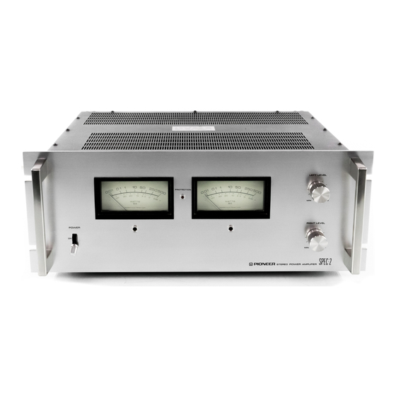
Pioneer SPEC-2 Service Manual - Page 6
Browse online or download pdf Service Manual for Amplifier Pioneer SPEC-2. Pioneer SPEC-2 50 pages. Pioneer spec-2 stereo power amplifier operating instructions
Also for Pioneer SPEC-2: Operating Instructions Manual (17 pages)

4. CIRCUIT DESCRIPTION
4 . 1 P O W E R A M P L I F I E R
The SPEC-2 is a high power design, employing a
cascoded differential amplifier first stage, push-pull
drive, and darlington triple push-pull circuit with
all stages direct coupled (OCL).
The circuit diagram is shown in Fig. 2. Q1 and Q2
form the differntial
amplifier. The input signal is
applied to Q1 and NFB from the output stage
applied to Q2 base. These two transistors are con-
nected in common base circuits with Q3 and Q4,
forming a cascode amplifier. Since the common
emitter circuit (Q1 & Q2) load becomes the input
of the following common base circuit stage, load
impedance is low and stable amplification can be
achieved.
Q3 and Q4 outputs drive Q5 and Q6 in opposite
phase. The Qb output via Q7 is applied to the
current mirror circuit formed by D2 and Q8, where
the phase is again inverted. Q6 and Q8 outputs
thus become signals of the same phase and perform
a pre-driver function.
The cunent mirror circuit is depicted in Fig. 1.
Current flowing through R2 and Q8 becomes equal
to that flowing through Rl and D2. In other words,
since R1 and R2 are equal, and the characteristics
of. D2 and Q8 base-emitter are also equal, the
current +BL reaching point A (in Fig. 1) through
R1 and D2 is equal to that reaching the same point
through R2 and Q8 base-emitter. This becomes
equivalent to having Q5 output directly driving
Q8.
I I I P U T H
By adopting this current mirror
circuit, when
muting relay RLb is OFF Q8 is cut off, Q10 - Q20
are switched OFF in succession, and operation
stops. The reversed phases of Q8 and Q6 outputs
cause them to cancel each other, reducing pop
noise and muting relay switching noise.
Q13 and Q14 in the following driver stage drive
the power transistors by direct coupling. The final
stage is a high output design with three power
transistors for each channel coupled in parallel.
This parallel coupling permits comparatively large
current (Ic) to be employed through each tran-
sistor, plus selection of an operating point with
good linearity and high amplification (hfe).
+ B l
l l : t 2
- llrirel
€
Fig. 1 Current Mirror Circuit
tu
Fig. 2 Power Amplifier Circuit
