Digilent Nexys2 Referentiehandleiding - Pagina 16
Blader online of download pdf Referentiehandleiding voor {categorie_naam} Digilent Nexys2. Digilent Nexys2 18 pagina's.

Nexys2 Reference Manual
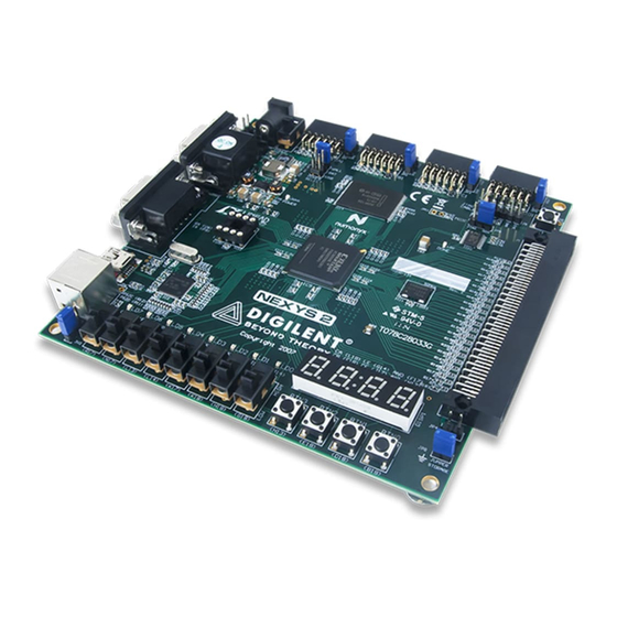
Expansion connector
The Nexys2 board includes a Hirose FX-2 high-
density 100 pin connector that is suitable for
driving peripheral boards with signal rates in
excess of 100 MHz. Many connector signals are
routed to the FPGA as differential pairs, and 47
connector pins are tied to ground, resulting in a
very low-noise connection system. The self-
aligning Hirose FX-2 connector can be used for
board-to-board connections or board-to-cable
connections using the mating Hirose FX2-100S-
1.27 available from many catalog distributors
and directly from Digilent.
All signals routed from the FPGA to the FX-2
connector include 75-ohm series resistors. The
table on the right shows all signal connections
between the FX-2 connector and the FPGA.
Signals without corresponding entries in the
FPGA column are not directly connected to the
FPGA.
Copyright Digilent, Inc.
Table 4: Hirose FX2 Connector Pin Assignments
J1A
Name
VCC3V3
1
2
VCC3V3
3
TMS
4
JTSEL
5
TDO-FX2
6
FX2-IO1
7
FX2-IO2
8
FX2-IO3
9
FX2-IO4
10
FX2-IO5
11
FX2-IO6
12
FX2-IO7
13
FX2-IO8
14
FX2-IO9
15
FX2-IO10
16
FX2-IO11
17
FX2-IO12
18
FX2-IO13
19
FX2-IO14
20
FX2-IO15
21
FX2-IO16
22
FX2-IO17
23
FX2-IO18
24
FX2-IO19
25
FX2-IO20
26
FX2-IO21
27
FX2-IO22
28
FX2-IO23
29
FX2-IO24
30
FX2-IO25
31
FX2-IO26
32
FX2-IO27
33
FX2-IO28
34
FX2-IO29
35
FX2-IO30
36
FX2-IO31
37
FX2-IO32
38
FX2-IO33
39
FX2-IO34
40
FX2-IO35
41
FX2-IO36
42
FX2-IO37
43
FX2-IO38
44
FX2-IO39
45
FX2-IO40
46
GND
47
FX2-CLKOUT
48
GND
49
VCCFX2
50
VCCFX2
Page 16/17
Digilent
www.digilentinc.com
FPGA
J1B
Name
1
SHIELD
2
GND
D15
3
TDO-ROM
4
TCK
5
GND
B4
6
GND
A4
7
GND
C3
8
GND
C4
9
GND
B6
10
GND
D5
11
GND
C5
12
GND
F7
13
GND
E7
14
GND
A6
15
GND
C7
16
GND
F8
17
GND
D7
18
GND
E8
19
GND
E9
20
GND
C9
21
GND
A8
22
GND
G9
23
GND
F9
24
GND
D10
25
GND
A10
26
GND
B10
27
GND
A11
28
GND
D11
29
GND
E10
30
GND
B11
31
GND
C11
32
GND
E11
33
GND
F11
34
GND
E12
35
GND
F12
36
GND
A13
37
GND
B13
38
GND
E13
39
GND
A14
40
GND
C14
41
GND
D14
42
GND
B14
43
GND
A16
44
GND
B16
45
GND
46
FX2-CLKIN
D9
47
GND
48
FX2-CLKIO
49
VCCFX2
50
SHIELD
Doc: 502-134
FPGA
A17
B9
M9
