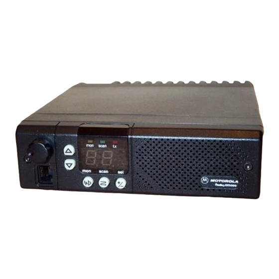
Motorola RADIUS GM300 Instrukcja serwisowa - Strona 37
Przeglądaj online lub pobierz pdf Instrukcja serwisowa dla Radio Motorola RADIUS GM300. Motorola RADIUS GM300 49 stron. 16-channel, conventional fm radio
Również dla Motorola RADIUS GM300: Instrukcja serwisowa (28 strony), Instrukcja obsługi (18 strony), Instrukcja obsługi (19 strony), Podręcznik użytkownika (37 strony), Instrukcja obsługi (2 strony)

Theory of Operation
RF Power Amplifiers
The third stage, Q2530, is the Class C RF Þnal power
ampliÞer. It provides 8.75 dB of gain and an output
power of up to 15 watts. Collector voltage is supplied
from UNSW B+ via a 0.2 ohm resistor, R2570. By mea-
suring the voltage drop across this resistor, the power
control circuit compensates for variations in Q2530Õs
collector current.
The antenna switch consists of two pin diodes, CR2550
and CR2551. L2553 is parallel-resonant with the off
capacitance of CR2550, increasing the diodeÕs isolation
when turned off. C2555 is a DC block. L2552 and
C2551, combined with the ÒonÓ inductance of CR2551,
form a series resonant circuit to lower the shunt imped-
ance presented by CR2551 when it is turned on.
In the receive mode, both diodes are off. Signals
applied at the antenna jack J1 are routed, via the har-
monic Þlter, through network L2551, C2552 and C2553
to the receiver input. In the transmit mode, 9.6T is
present and both diodes are forward-biased into con-
duction. The transmitter RF from Q2530 is routed
through CR2550, and via the harmonic Þlter to the
antenna jack. CR2551 conducts, shunting RF power
and preventing it from reaching the receiver. L2551 is
selected to appear as a 1/4 wave at UHF, so that the
low impedance of CR2551 appears as a high imped-
ance at the junction of CR2550 and the harmonic Þlter
input.
The harmonic Þlter is a seven pole 0.1 dB ripple Cheby-
chev low pass Þlter with a 3 dB frequency of approxi-
mately 700 MHz and less than 1 dB insertion loss.
10-25 Watt UHF Power Amplifier
The 10-25 watt UHF power ampliÞer is designed to
cover the range of 438-470 MHz and has four stages.
The Þrst stage, Q2610, operates in Class A with base
bias from 9.6T. It provides 11.8 dB of gain and an out-
put of 300 milliwatts.
The second stage, Q2620, has a nominal gain of 8.2 dB
and power output of up to 2 watts. The output of this
stage is adjusted by the controlled B+ voltage which
supplies its collector.
The third stage, Q2630, operates in Class C with 8.1 dB
gain and a power output of up to 13 watts. Collector
voltage is directly from UNSW B+.
The fourth stage, Q2640, is the Þnal RF power ampli-
Þer, which operates Class C directly from UNSW B+. It
provides up to 30 watts output. Collector current is
monitored by the power control circuit by measuring
the voltage drop across a .05 ohm resistor, R2670, in
series with the collector DC supply lead.
The antenna switch consists of two pin diodes, CR2650
and CR2651. L2652 and C2651-2, combined with the
ÒonÓ inductance of CR2651, form a series resonant cir-
cuit to lower the shunt impedance presented by
2-12
CR2651 when it is turned on. In the receive mode, both
diodes are off. Signals applied at the antenna jack J1 are
routed, via the harmonic Þlter, through network L2651,
C2652 and C2653 to the receiver input. In the transmit
mode, 9.6T is present and both diodes are forward-
biased into conduction. The transmitter RF from Q2640
is routed through CR2650, and via the harmonic Þlter
to the antenna jack. CR2651 conducts, shunting RF
power and preventing it from reaching the receiver.
L2651 is selected to appear as a 1/4 wave at UHF, so
that the low impedance of CR2651 appears as a high
impedance at the junction of CR2650 and the harmonic
Þlter input.
The harmonic Þlter is a seven pole 0.1 dB ripple Cheby-
chev low pass Þlter with a 3 dB frequency of approxi-
mately 500 MHz and less than 1 dB insertion loss in the
passband.
25-35/40 Watt UHF Power Amplifiers
There are four high-power UHF ampliÞers, which pro-
vide 25-40 watts output in the 403-433, 438-470 or 465-
490 MHz bands, or 25-35 watts output in the 490-520
MHz band. All have four stages and are similar in cir-
cuitry and layout.
The Þrst stage, Q2710, operates in Class A with operat-
ing voltage obtained from 9.6T. The second stage,
Q2720, is a gain- controlled Class C stage, the output
power of which is adjusted by varying the controlled
B+ collector DC supply. The third stage, Q2730, oper-
ates in Class C with collector voltage obtained directly
from UNSW B+. The fourth stage, Q2740, is the Þnal RF
power ampliÞer, which operates Class C directly from
UNSW B+. SpeciÞc operating parameters are:
Range
403-433
Stage 1
Gain:
11.8 dB
P
:
300 mW
OUT
Stage 2
Gain:
8.2 dB
P
:
2 W
OUT
Stage 3
Gain:
8.1 dB
P
:
13 W
OUT
Stage 4
Gain:
5.9 dB
P
:
50 W
OUT
Collector current of the Þnal stage is monitored by the
power control circuit by measuring the voltage drop
across a .01 ohm resistor, R2770, in series with the col-
lector DC supply lead.
The antenna switch consists of two pin diodes, CR2750
and CR2751. L2753, when used, is parallel-resonant
with the off capacitance of CR2750, increasing the
diodeÕs isolation when turned off. C2755 is a DC block,
present if L2753 is used. L2752 and C2750-1, combined
68 No.
Name of Manual
438-470
465-495
490-520
11.8 dB
10 dB
10 dB
300 mW
200 mW
200 mW
8.2 dB
9.5 dB
9.5 dB
2 W
1.8 W
1.8 W
8.1 dB
8.5 dB
8.5 dB
12.9 W
13 W
13 W
6.1 dB
6.3 dB
5.7 dB
52.8 W
55 W
48 W
March, 1997
