EPC EPC9144 Manual de início rápido - Página 3
Procurar online ou descarregar pdf Manual de início rápido para Placa-mãe EPC EPC9144. EPC EPC9144 9 páginas. Development board for a 15 v high current pulsed laser diode driver
QUICK START GUIDE
OPERATING PRINCIPLE
THE EPC9144 is intended as both a demonstration board and a flexible
development platform. It is functional out of the box, but is designed
to be easily modified to accommodate a broad range of applications.
It is highly recommended that the user read the entire guide, but
especially the section MODIFICATIONS, in order to get maximum
value from the EPC9144.
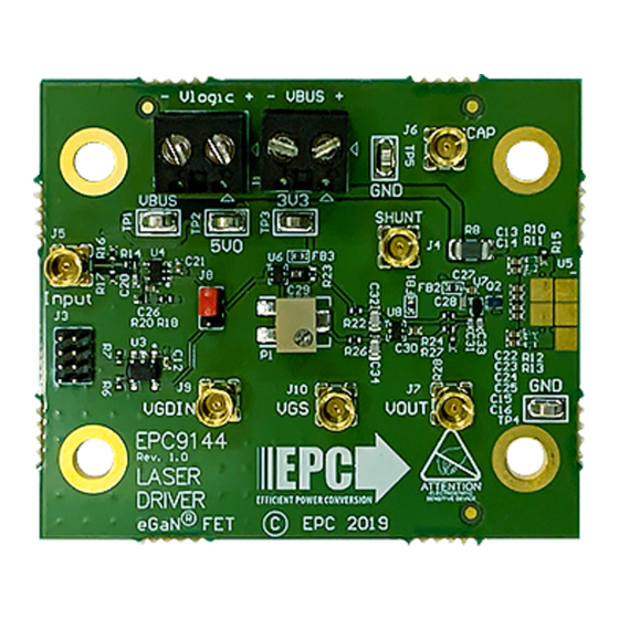
The EPC9144 is shipped as a rectangular pulse laser diode driver. Please
refer to the block diagram (Fig. 2) and the schematics (Figures 7 & 8).
It has several possible modifications (section MODIFICATIONS), but only
the basic operation will be covered in this section. The EPC9144 basic
operating principle is to act as a current gate to allow current from the
voltage bus to flow through the laser diode or other load when the FET
Q1 is turned on, and stop the load current when the Q1 is turned off.
The speed of the driver and FET means that turn-on and turn-off can be
accomplished as fast as 500 ps and 250 ps, respectively, even for load
currents of approximately 10 A.
The FET Q1 is controlled via an input pulse that is delivered to MMCX
connector J5, which is terminated on the demo board with 50 Ω. J5 is
followed by a logic level translator. As shipped, the level translator is set
for 3.3 V logic levels, but the EPC9144 may be modified to accommodate
other logic levels (See MODIFICATIONS for further details).
After the level translator, the input pulse goes through a narrow pulse
generator circuit. The input pulse should be set > 10 ns longer than the
desired output pulse. As shipped, the pulse width is set to approximately
5 ns, but it may be adjusted to values in the range of 1.2 ns to 20 ns via
trimpot P1, with the lower limit determined by the LMG1020 gate driver IC.
Please note that it is possible to reduce the adjust the input pulse to a
value below the minimum pulse width capability of the LMG1020 gate
driver. In this case, the output will fail to function properly, and the P1
adjustment must be increased. Finally, in the case where one wishes to
control the pulse width externally via the input pulse, the narrow pulse
generator may be bypassed as discussed in the section MODIFICATIONS.
When the input goes high, the gate driver turns on Q1, allowing current
flow through the laser diode or load U2. After the narrow pulse generator
output goes low, Q1 turns off. If there is current remaining in the power
loop inductance, diode-connected EPC2036 FET Q2 can conduct and
help prevent overvoltage of the laser and FET.
The voltage bus for the laser diode or other load is bypassed via the
capacitor bank {C22, C23, C24, C25}. This capacitor bank is part of the
main power loop inductance, and the layout is designed to minimize
the effect of resulting parasitic inductance. The capacitor bank is fed
through a relatively small resistance formed by {R10, R11, R12, R13}.
The resistance served to limit the laser or load current continuous value
in the case of long pulses, and also serves to damp parasitic resonance
of the power loop.
Measurements of key waveforms can be made through the MMCX test
points provided. These test points can provide waveform measurements
with equivalent bandwidths > 3 GHz. As a result, they have requirements
EPC – THE LEADER IN GaN TECHNOLOGY |
WWW.EPC-CO.COM
| COPYRIGHT 2019 |
V7in
Signal generator
Signal Generator
Pulse width
adjust
Figure 2: Connection and measurement setup
Figure 3: Output terminals of the EPC9144
and properties that differ from most conventional oscilloscope
probes. More details on the usage of these test points is provided in
section MEASUREMENT CONSIDERATIONS.
LASER DIODE OR LOAD CONSIDERATIONS
The EPC9144 can be used as is to mount a laser diode or other load.
Figure 3 highlights the output pad locations. However, many laser
suppliers have different mounting footprints, making it difficult to
optimize the performance of the driver and still maintain the desired
flexibility. The use of an interposer PCB provides a solution to this
problem with a small added performance penalty in the form of an
additional 50 pH to 100 pH power loop inductance. The EPC9144 ships
with the EPC9989 interposer PCB, shown in Fig. 4. The EPC9989 has
an assortment of 5 mm square interposer PCBs that can be snapped
off the board. These interposers have various footprints on the top
side that can accommodate several surface mount laser diodes, an
MMCX connector, and several patterns designed to accommodate a
wide variety of possible loads. These interposers mount between the
EPC9144 and the laser diode or other load. The EPC9989 is updated
as new lasers or loads become available, so Fig. 4 may not show the
latest board.
Demonstration System EPC9144
VBUS
V7
V
IN
BUS
– +
–
+
Note
Note polarity
Polarity
Laser anode
Laser cathode
(FET drain)
GND (for alternate
applications)
Laser
diode
or load
Oscilloscope
(50 inputs)
| 3