Digilent Cmod S6 Manual de referência - Página 3
Procurar online ou descarregar pdf Manual de referência para Placa-mãe Digilent Cmod S6. Digilent Cmod S6 5 páginas. Fpga board

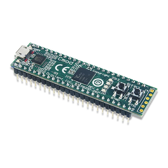
Cmod S6™ FPGA Board Reference Manual
5
Quad SPI Flash Memory
The Cmod S6 includes a non-volatile 16Mbyte Spansion Quad SPI Flash that can store FPGA configuration files as
well as user data. The Spansion device supports the standard 4-wire SPI protocol, as well as the newer Quad I/O
and Dual I/O protocols at speeds from 50 MHz to 133 MHz, depending on the protocol and command used. For
more information on the SPI Flash memory, please see the "S25FL128S and S25FL256S Data Sheet" at
www.spansion.com.
To achieve the fastest programming speed over the Digilent USB-JTAG connection, when generating the bitstream
in Project Navigator, change the SPI bus width to four and enable bitsream compression. To do this, simply select
"Generate Programming File" and navigate to Process>Process Properties. In the pop-up menu, enable –g
Compress under "Synthesis Options" and set –g SPI_buswidth to four under "Configuration Options".
6
Digilent EPP Interface
The Cmod S6 implements the Digilent EPP interface (DEPP) for 8-bit parallel data transfers between the FPGA and
a computer attached via the USB Micro connector. DEPP is based on a set of APIs available in the Adept 2 public
SDK, available from the Adept product page at www.digilentinc.com. These APIs work in concert with firmware
running on the USB controller to provide a high-level software interface for transporting data between a PC and
the Cmod S6.
To use the DEPP interface, the host PC must use software built from the Adept SDK DEPP libraries, and the FPGA
has to be running a configuration that implements a DEPP controller. For a description of the DEPP library API,
refer to the "DEPP Programmer's Reference Manual" included with the Adept 2 SDK. For information on designing
a DEPP controller, refer to the "Digilent Asynchronous Parallel Interface (DEPP)" document, also included with the
Adept 2 SDK.
7
Factory Loaded User Demo
The Quad SPI Flash is loaded with a configuration file at the factory. When powered on, the file will configure the
FPGA such that the buttons control the states of two LEDs, while the other two LEDs toggle at a speed of about 1
Hz. The general purpose I/O pins are initially configured as inputs, and are pulled up internally by the FPGA to read
a logic level '1'. Each individual pin can be controlled using the DEPP interface to either drive the pin as an output,
or to read the logic level that is present on the pin as an input.
The I/O pins can be controlled by writing to specific DEPP register addresses. To test the interface, the "Register
I/O" tab within the Adept 2 application can be used. Table 1, shown below, gives a description of register
addresses and functions.
Copyright Digilent, Inc. All rights reserved.
Other product and company names mentioned may be trademarks of their respective owners.
Page 3 of 4
