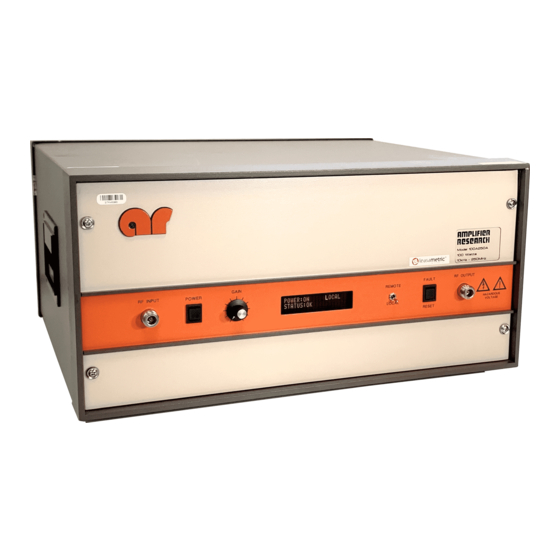
Amplifier Research 100A250 series Руководство - Страница 12
Просмотреть онлайн или скачать pdf Руководство для Усилитель Amplifier Research 100A250 series. Amplifier Research 100A250 series 19 страниц.

Model 100A250A
3.1
INTRODUCTION
The Model 100A250A amplifier consists essentially of a push-pull output stage of broadband MOSFET transistors
driven by a 10 watt driver amplifier. Overall power gain of the amplifier is a minimum of +50dB for 1 milliwatt
input. Input and output impedance matching circuits are utilized to provide optimum power transfer of the RF signal
when the amplifier is connected to source and load impedance of 50 ohms. Combined with negative feedback at
each stage and factory aligned equalizers, this provides an overall flat frequency response.
The self contained power supply consists of three switching power supplies. Two of the supplies are connected in
series to provide 30 volts for the final amplifier. This voltage is further regulated down to 28 volts for the driver
amplifier. The third supply is used to supplies ± 12VDC and +5VDC to power the operate/control and the gain
control. The three power supplies operate at line voltages of 90 to 132 VAC and 180 to 264 VAC, 50/60 Hz
selected automatically.
3.2
DRIVER AMPLIFIER SECTION
Refer to "Schematic Diagram Number 1003958, RF Board Assembly".
The input signal is fed through the gain control assy to the gate of Q1, which is limited by diodes CR2 and CR3.
Gate bias for Q1 is supplied through R14 and adjusted by R10. The output of Q1 is coupled through C8 to the
equalizing network R32, R33, R34 L15 and C36. The output of the equalizing network is coupled through C4 to the
gate of Q3. Resistor R12 and capacitor C12 provide adjustments for response tuning. Gate bias for Q3 is supplied
through R13 and adjusted by R8.
The output of Q3 is coupled through transformer T1, which drives the push-pull stage Q4 and Q5. Resistor R22 is
used to adjust the bias voltage for both Q4 and Q5, in conjunction with R23 which is used to balance the push-pull
operation. The output of Q4 and Q5 are coupled through matching transformer T2 to a coaxial connector, which is
the driver's output.
3.3
FINAL AMPLIFIER SECTION
Refer to "Schematic Diagram Number 1007520, RF Board Assembly, Final Amp".
The input signal is applied to coax connector J1. The signal then goes to an equalizer network consisting of C1, C2
and L1 which is used for adjusting the flatness. The signal is then conducted to transformers T1 and T2 which
provide impedance matching to the push pull transistors Q1A and Q1B. The bias voltage is adjusted with R12, while
the balance between the transistors is adjusted with R10. The output of Q1A and Q1B are coupled through matching
transformers T3 and T4 to the output connector on the front panel.
Over current protection is provided by U1, U2, U3 and U4, by sensing the input current and lowering the bias
voltage if the current goes above the normal operating level.
SECTION III
THEORY OF OPERATION
Manual Text
3-1
REV -
