Broadcom ACPL-336J Справочное руководство - Страница 9
Просмотреть онлайн или скачать pdf Справочное руководство для Материнская плата Broadcom ACPL-336J. Broadcom ACPL-336J 16 страниц. Fuji electric small pim module (m728/m732) evaluation board

ACPL-336J Reference Manual
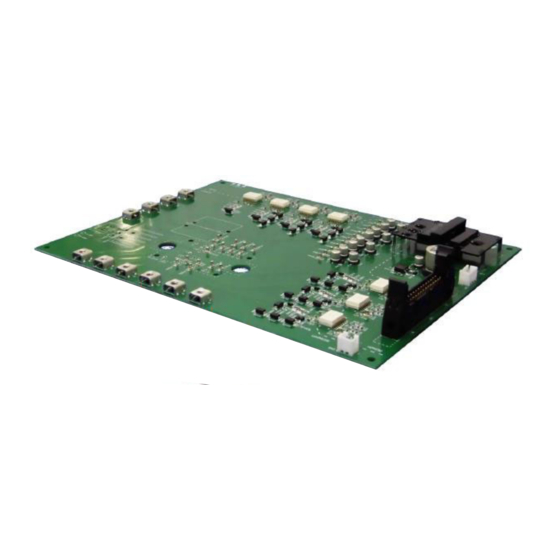
Fuji Electric Small PIM Module (M728/M732) Evaluation Board
The ACPL-336J has an integrated input LED driver with high impedance input (VIN+) for interfacing with the controller. The
LED driver's output (VLEDDRV) must be connected with the recommended split resistors to LED1 to achieve the rated high
CMR performance of more than 50kV/µs. If the LED driver is not used, LED1 can still be driven directly by other means of
discrete driver configuration.
It is recommended that the two resistors (R14/R15) connected to input LED's anode and cathode are split in the ratio 1:1.
They will help to balance the common mode impedances at the LED's anode and cathode. This helps to equalize the
common mode voltage changes at the anode and cathode to give high CMR performance. In this case, R14 and R15 are
150Ω resistors to limit LED1 current to about 10 mA based on 5V VCC1 supply.
The primary side has two open drain FAULT and UVLO feedback outputs suitable for wired 'OR' applications. ACPL-336J
monitors the output power supply constantly. When secondary side power supply is lower than undervoltage lockout (UVLO)
threshold, the gate driver output will shut off to protect IGBT from low voltage bias. The low output power supply fault will be
reported through the UVLO feedback. In this way, the UVLO feedback can also serve as a READY signal to the controller
during power up. These open drain FAULT and UVLO outputs are connected to 10 kΩ pull-up resistors (R12/R13) and
330 pF filtering capacitors (C12/C13).
The supplies, VCC1 and VCC2 are connected to C11, C101, C103 and C104 (1 µF) bypass decoupling capacitors to provide
the large transient currents necessary during a switching transition.
The ACPL-336J monitors the saturation (collector) voltage of the IGBT and triggers a local shutdown sequence if the
collector voltage exceeds a predetermined threshold of 7V during short circuit or over current fault condition. The DESAT
pin is connected to the collector of IGBT (P1) via 600V high voltage blocking diodes, D103, D104, D105, and resistor R101
(1 kΩ). Blanking capacitor, C102 (470 pF) is used to prevent false fault detection by filtering high frequency noise transient.
The VCLAMP pin is connected directly to the gate of the IGBT and can sink 2.5A of parasitic Miller current during switching
to prevent false turn on of the IGBT.
The gate resistors R102 (15Ω) and R103 (0Ω) serve to limit gate current and indirectly control the IGBT switching time.
Diode, D108, is used to bypass resistor R103 and control the gate current and slew rate during IGBT gate discharging. It
should be noted that the gate resistor must limit ACPL-336J peak output current to within 2.5A absolute maximum.
This negative going voltage spike is typically generated by inductive loads or reverse recovery spike of the IGBT
freewheeling diodes. Zener diode, D101, and Schottky diode, D101, are used to prevent a false fault signal caused by
positive and negative spikes.
Broadcom
ACPL-336J-RM100
9
