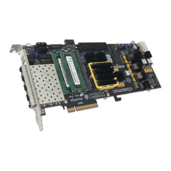
Digilent NetFPGA-SUME Справочное руководство - Страница 16
Просмотреть онлайн или скачать pdf Справочное руководство для Материнская плата Digilent NetFPGA-SUME. Digilent NetFPGA-SUME 20 страниц.

NetFPGA-SUME™ Reference Manual
Virtex-7 FPGA is the master on the I
2
C bus, and connected to an I
2
C multiplexor (PCA9548) via a level shifter
(FXMA2102). The PCA9548 has 8 downstream ports which are wired to SFP+ transceivers, DDR3 SODIMMs, FMC
connectors, any-frequency precision clock generator (SI5324), and the PMBus (a subset of I
2
C protocol) interface of
power management chips (LTC2974). In the figure, the hexadecimal numbers on the double arrow is the control
register value to select the corresponding downstream port, and the red hex number besides each device is the I
2
C
slave address of each device.
5.7
Clocking
On-board oscillators and clock generators support various board subsystems. Transceivers connected to SFP+
interfaces (Bank 119) and QTH connectors (Bank 117, 118) share the same SFP_CLK (Bank 118 Clk0) generated by
an any-frequency precision clock multiplier/jitter attenuator (IC20 SI5324). Under most cases when SFP+ interfaces
are configured to be 10Gb Ethernet ports, the output clock frequency of SI5324 is set to be 156.25MHz (Please
refer to reference design in NetFPGA-SUME repository for recommended configuration values). The transceivers
for both SATA connectors (Lane 0, 1 Bank 116) run from a 150MHz SATA_CLK (Bank 116 CLK0) generated by a low-
jitter LVDS Oscillator (IC21 DSC1103). FPGA_SYSCLK (system clock for FPGA), QDRII_SYSCLK (shared by QDRII+
memory A and B), QDRIIC_SYSCLK (used by QDRII+ memory C) are 200MHz clocks generated by another low-jitter
LVDS Oscillator (IC16 DSC1103) level-shifted by a low-jitter low-skew clock buffer (IC17 SI5330). DDR3_SYSCLK
(shared by two DDR3 SODIMMs) is a 233.33MHz clock generated by the third low-jitter LVDS oscillator (IC18
DSC1103). The PCIE-CLK needs external 100MHz clock used specifically for PCI-Express Gen3 x8 design and
FMC_GBT_CLK0/1, FMC_CLK0/1 connected to FMC connectors reserved for user-defined FMC peripheral boards.
The following table is a summary for all the clock resources available on board:
Copyright Digilent, Inc. All rights reserved.
Page 16 of 18
Other product and company names mentioned may be trademarks of their respective owners.
